The past industrial revolutions liberated humans from animal power, made mass production possible, and accelerated human welfare across markets and territories. According to Prof Klaus Schwab, Founder and Executive Chairman of The Word Economic Forum, the Fourth Industrial Revolution (4IR) is “characterized by a range of new technologies that are fusing the physical, digital and biological worlds, impacting all disciplines, economies and industries and even challenging ideas about what it means to be human”.
The resulting shifts and disruptions mean that we live in a time of great promise and great peril. The world has the potential to connect billions more people to digital networks, dramatically improve the efficiency of organizations and even manage assets in ways that can help regenerate the natural environment, potentially undoing the damage of previous industrial revolutions.
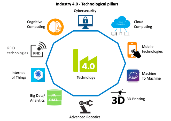
The Fourth Industrial Revolution is marked by emerging technology breakthroughs in different field which include
- Robotics
- Artificial Intelligence
- Blockchain
- Quantum Computing
- Nanotechnology
- Additive Manufacturing
- Internet Of Things
- Electric and Autonomous Vehicles
- 5G Wireless Technologies
- Biotechnology
President Cyril Ramaphosa of South Africa, knowing the immense benefits which the Fourth Industrial Revolution will play in accelerating growth and development of his nation, recently launched a 30-man Presidential Commission on the Fourth Industrial Revolution which will identify relevant policies, strategies and action plans that will position South Africa as a globally competitive economy in the 4IR.
South African President Cyril Ramaphosa on Tuesday appointed 30 members of the Presidential Commission on the Fourth Industrial Revolution (4IR), the Presidency has said in a statement.
“The commission will assist government in taking advantage of the opportunities presented by the digital industrial revolution,” the Presidency said in a statement on Tuesday.
On Thursday April 11th 2019, Communications Minister of Republic Of South Africa will unveil the 4th Industrial Revolution in South Africa, in partnership with Telkom, a leading telecom solutions provider in the country, Universities of Witwatersrand and Fort Hare, and the City Of Johannesburg. This partnership which will help to create a national dialogue is aimed at creating a framework for maximizing the potentials of the 4IR. Besides, it will also complement and support national activities relating to the Fourth Industrial Revolution.
More so, the South African Parliament recently held an exhibition in partnership with the Department of Science and Technology tagged ‘’4th Industrial Revolution: Demonstrating South Africa’s Readiness’’ to deepen its understanding on this technological trajectory that will redesign economies, industries and markets,
Nigeria should learn from South Africa and change the composition of its Presidential Council on Research and Innovation and saturate it with skilled innovators and technocrats instead of politicians. By doing this, the experts will have the opportunities to fashion out an implementable roadmap for the Fourth Industrial Revolution to the benefits of all Nigerian citizens.
Yes, Nigeria must develop capabilities in this revolution to have any chance of competing in Africa. South Africa has a clear vision; Nigeria must elevate its game as it relates with technologies of the future. If you check very well, the ANC flag has the wheel of industry: now, they want to move it really fast to drive their economy. That is amazing thing to do now that everything is about technology.