

Introduction
Most modern entertainment gadgets, equipment and tools incorporate integrated circuits that perform some specific functions that make the entertainment experience fascinating for users. From the simple toys for toddlers to the complex game studios in casinos, hardware forms a major component of entertainment technology. With the advent of integrated circuits, and subsequent development of CMOS (complementary oxide semiconductor) technologies, there has been remarkable success in the number of application specific integrated chips (ASIC) tailored for gaming and general entertainment. And from programmable micro-controllers to field programmable gate arrays (FPGAs), chips are common tools to both computer scientist and engineer. Consequently, understanding the fascinating processes used in making these chips which are programmed and used in circuit boards could be interesting for all stakeholders in the field of entertainment technology. The design of integrated circuit is perhaps one of the most complex stages in the development process of game and entertainment infrastructure forming a vital part of the entertainment technology. Increasingly, chip designers are discovering ways of implementing functions hitherto done with massive codes of computer programs inside integrated circuits.
Integrated circuits are circuits that could contain millions of transistors and other circuit elements on a single die (a piece of silicon that contains active devices and input and output interfaces) [1]. They are made on special materials called semiconductors with silicon and gallium arsenide (GaAs) the most common. Its evolution is a major milestone in the history of modern industry as it has driven a revolution in computing capability due to a long trend in performance, density gains, and cost with scaling [1,2]. Remarkably, these circuits could be made using different technologies. But over time, complementary metal oxide semiconductor (CMOS) technology has become the industry de-facto and the most prevalent method of choice. Its major advantages over other technologies are its ease of integration of circuit components and low static power consumption [3]. This is the main technology used to make analog-to-digital converters, micro-controllers, FPGA (an integrated circuit that contains an array of identical cells with programmable interconnections), microprocessors and host of others that are used while developing entertainment hardware. Its continuous improvements has driven reduction in size of game gadgets, better performance, more efficient battery management for battery operated devices, cost as well as hardware ergonomics.
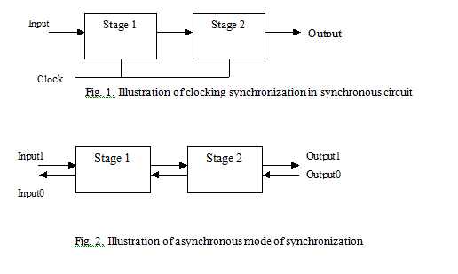
Integrated circuit could be digital, analog or mixed signal (a combination of both analog and digital). While the digital chip involves designing at logic levels of 1 and 0, the analog is based on continuous signal. Besides, sequencing and communication synchronization on chip could be done by use of globally distributed clocks for synchronous designs or local handshaking variables for asynchronous designs. Between these two methods, the former is the more common method. However, issues like switching delay, complexity management and clock distributions, which may place limitation on synchronous chip performance with an acceptable level of reliability as technology is scaled down, had stimulated interests in the study of asynchronous systems [4,5]. Asynchronous chips are known as self timed circuits since they do not use clocks but rather use local variables that perform the functions of handshaking requests and acknowledgements. Design of asynchronous digital system involves an entirely different concept when compared to synchronous design. The idea of clockless system introduces so many design parameters, which must be tracked as the requests, and acknowledgements signals are generated and routed. The initial stage of asynchronous system development would interest a computer scientist because of enormous digital “coding” that describes level of system abstraction.
For an illustration of the two design techniques, consider Fig. 1 where a signal, clock, is used to coordinate the functional operations of the circuit. The clock signal enables the circuit to manage the beginning of an operation, its termination and the beginning of another one and so on. Correct functionality of this circuit partly depends on the clock and any problem with this signal could potentially affect the accuracy of the functions being performed. On the other hand, consider Fig.2 where there is no clock signal. Rather, local signals, called handshake signals (actually request and acknowledgement signals), are used to coordinate when an operation has started, terminated and so forth. The implication is that subsequent operations must wait until the proceeding ones have started and completed based on design without regard to any global control signal. However, this usually comes at the expense of more wiring. For this article, I will focus on the synchronous system due to its popularity.
Integrated Circuit Design Flow
The process of chip design is very complex and its understating requires many years of study and practical experience. From a digital integrated circuit design perspective, it could be divided into different hierarchies as shown in Fig.3 where the problems are examined at several different levels [6].
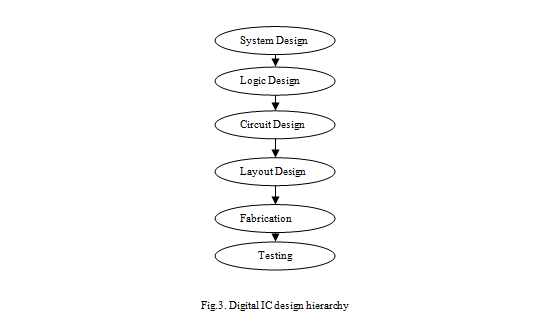
System Design: This stage provides the specifications and main operations of the chip. It examines such issues like chip area, power, functionality, speed, cost and other design factors while setting these specifications. Sometimes, the resources available to the designer could act as a constraint during this stage. For instance, a designer may like to design a chip to work at 1.2V, but available process technology can only support a voltage of 5V. In this situation, the designer has to adjust these specifications to satisfy the available tools. It is always a good habit to understand the process technology available before system design and specifications. Process technology is basically the specific foundry technology rules where the chip would be fabricated. Typical examples are AMI 0.5um, TSMC 0.35um and IBM 0.13um. A design based on one process technology is unique to that process and accordingly should be fabricated in a foundry that supports that process. At the system design level, the main sections of the system are illustrated with block diagrams, with no details on the contents of the blocks. Only the input and output characteristics of the sections are detailed [6].
Logic Design: At this stage, the designer implements the logic networks that would realize the input and output characteristics specified in the previous stage. This is generally made of logic gates with interconnecting wires that are used to realize the design.
Circuit Design: Circuit design involves the translation of the various logic networks into electronic circuitries using transistors. These transistors are switching devices whose combinations are used to realize different logic functions. The design is tested using computer aided design (CAD) tools and comparisons are made between the results and the chip specifications. Through these results, the designer could have an idea of the speed, power dissipation, and performance of the final chip. An idea of the size of the chip is also obtained at this stage since the number of transistors would determine the area of the chip. Experienced designers optimize many design variables like transistor sizes, transistor numbers, and circuit architecture to reduce delay, power consumption, and latency among others. The length and width of the transistors must obey the rules of the process technology.
Layout Design: This stage involves the translation of the circuit realized in the previous stage into silicon description through geometrical patterns aided by CAD tools [3,6]. This translation process follows a process rule that specifies the spacing between transistors, wire, wire contacts and so on. Violation of these rules results to malfunctioning chips after fabrication. Besides, the designer must ensure that the layout design accurately represents the circuit design and that the design is free of errors. CAD tools enable checks for errors and also incorporate ways of comparing layout and circuit designs provided in form of Layout Versus Schematic (LVS) checks. When errors are reported, the designer has to effect the corrections. A vital fundamental stage in layout design is Extraction, which involves the extraction of the circuit schematic from the layout drawings. The extracted circuit provides information on the circuit elements, wires, parasitic resistance and capacitance (a parasitic device is an unbudgeted device that inserts itself due to interaction between nearby components). With the aid of this extracted file, the electronic behavior of the silicon circuit is simulated and it is always a good habit to compare the results with the system specification since this is one of the final design stages before a chip is sent to the foundry.
Fabrication: Upon satisfactory verification of the design, the layout is sent to the foundry where it is fabricated. The process of chip fabrication is very complex. It involves many stages of oxidation, etching, photolithography, etc. Typically, the fabrication process translates the layout into silicon or any other semiconductor material that is used. The result is bonded with pins for external connections to circuit boards.
Fabrication process uses photolithographic masks, which define specific patterns that are transferred to silicon wafers (the initial substrate used to fabricate integrated circuits) through a number of steps based on the process technology. The starting material, the wafer, is oxidized to create insulation layer in the process. It is followed by photolithographic process, which involves deposition of photoresist on the oxidized wafer, exposure to ultra-violet rays to form patterns and etching for removal of materials not covered by photoresist. Ion implantation of the p+ or n+ source/drain region and metallization to form contacts follow afterwards. The next stage is cutting the individual chip from the die. For external pin connection, bonding is done. It is important to emphasize that this process steps could be altered in any order to achieve specific goals in the design process. In addition, many of these functions are done many times for very complex chips. Over the years, other methods have emerged. A notable one is the use of insulators (like sapphire) as starting materials instead of semiconductor substrate (the silicon on which active devices are implanted) to build the transistors. This method called Silicon on Insulator (SOI) minimizes parasitic in circuits and enable the realization of high speed and low power dissipation chips [6].
Testing: The final stage of the chip development is called testing. Electronic equipment like oscilloscopes, probes, pattern generators and logic analyzers are used to measure some parameters of the chip to verify its functionalities based on the stated specifications. It is always a good habit to test for various input patterns for a fairly long time in order to discover possible performance degradation, variability, or failures. Sometimes, fabricated chip test results deviate from simulated results. When that occurs, depending on application, the designer could re-engineer the circuit for improvement and error corrections. The new design should be fabricated and tested at the end.
A Case study
For simplicity, let us imagine the design of a simple chip that would enable an addition of player’s score during a video game. One vital component of that chip would be an arithmetic logic unit (ALU). Many ALU have adder circuits inside. We would use the design of a simple full adder to illustrate the design process discussed above. This is a trivial design and in no way a representative of the level of work in state of the art digital circuits used in computers, games, etc.
System Design: The truth table of a full adder is presented in Table 1. There are two digital inputs and a carry-in bit. The sum and carry are the results of the adder based on the sequence of inputs. The implementation is on CMOS 0.6um (minimum transistor length of 0.6 micrometer) and the voltage levels are 5V(Vdd) and 0V(GND). In digital logic, these are represented as 1 (high voltage) and 0 (low voltage) respectively. We could specify the maximum power dissipation and speed if the design is very complex at this stage. Sum and Carry are obtained by digital addition of the input sequences as represented in the truthtable, a combination table that specifies the values of Boolean expression for all possible input sequences. Ability to build truthtable is very important in digital design since it enables the designer to evaluate all the input sequences with output results. It is a prerequisite to successful design of digital systems. For instance, when A=B=C=1, the addition of 1+1+1 = 3. Converting 3 to binary (base two) is 11. So we represent the Sum as 1 and Carry as 1. For input sequence of A=B=1 and C=0, the addition 1+1+0 =2 and converting 2 to base two gives 10. Hence, Sum takes 0 and Carry 1.


Logic Design: The logic implementation of the adder is given in Fig.4. This is the top-level entity with instantiated components of exclusive-OR (XOR), 2-input and 3-inputs NAND gates. Each of these components must be verified and tested as standalone before they can be used in the top-level. As shown in the figure, input sequence (A=1, B=0, C=1) will result to Sum =0, and Carry =1.
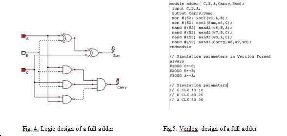
Alternatively, the logic design could be done with the aid of high-level description language such as VHDL (VHSIC Hardware Description Language, with VHSIC standing for Very High Speed Integrated Circuit) or Verilog. This offers a way of managing complexity associated with high performance systems on chip (SOC) as well as aid testing and verification of design before implementation in hardware. This is a smart strategy since it would be inconceivably impossible to implement state of the art microprocessor with millions of transistors using logic design. Such a method would be cumbersome, time consuming, ineffective and failure prone since it would be difficult for the designer to keep tracks of the design. For this reason, ability to “code” in VHDL or Verilog is a major skill required for all digital designers. Using these languages, a digital system is described in a textual format based on syntax used to specify gates and wires. It also offers specific delay information and hardware specific parameters that make design validation a lot easier. This design could be a structural, or behavioral description of the design. A Verilog design of the full adder is presented in Fig.5.
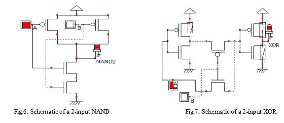
Circuit Design: The design of the full adder as noted above involves XOR and NAND gates. The circuit design would implement these designs in form of schematics using transistors. Understanding the behaviors of transistors, both the PMOS and NMOS is vital to designing and realizing these logic gates. The schematic design of 2-input NAND and XOR are presented in Fig.6 and Fig.7 respectively. To test these circuits, input sequences (A= 1, B=0) are applied to the circuits. The results shown are accurate based on the behavior of NAND and XOR gates. For NAND, input sequence of A=B=1 gives 0, while others input sequences return 1. NAND is a complement of AND, or in other words, an inverted AND (logic 1 is complement of logic 0 and vice versa). For XOR, input sequences (A=B =1; A=B=0) return 0 while others give 1. For the full adder, the complete schematics would incorporate all the schematics of the logic gates. Sizing of the transistors used in the design is very crucial as it does affect circuit performance.
Layout Design: The full adder is translated into a silicon description based on design rule specified by the CMOS 0.6um rule. Basically, every wire, transistor, contact or any section of the circuit could be represented by polygons of different materials. It could be metal for connection, poly (special type of silicon) for making transistors or via for contacts among others. The length and width of these polygons designate the sizes of circuit elements they represent. Fig. 8 shows a 2-D layout of the design, which is made up of many different layers, each represented by a different color. The blue sections represent different metal layers, while the red sections are a special type of silicon called poly-silicon. When a poly-silicon crosses a Select (a diffusion region), transistor is formed. The PMOS transistors are enclosed in a N-well since the starting substrate of the design is a p-substrate. Usually, many CAD tools have facilities that check for errors in the design based on the process technology. Any violation of the rule must be corrected in the layout. In an analog design, layout is more complex because of problems of parasitic and crosstalks (kind of interference in the system). Consequently, analog layout must be protected and shielded from sources of noise. Pad frame layout that provides input/output ports to the chip is shown in Fig. 9. The pads are stack of metal squares connected by contacts that surround the central core region with signal assignments for easy wiring access to the circuits. A better view of this layout is shown in a 3-D as shown in Fig.10. The figure shows the different layers of diffusion, oxide, etc that have been carried out to realize the circuit.
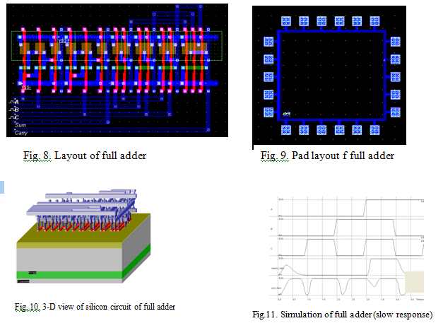
The verification of the layout is very important and crucial. After extraction of the layout, the result is simulated to check correctness in design. There are many ways this could be done depending on the nature of the design. It could be by checking the current, voltage levels and other circuit parameters for correctness. Fig. 11 is a simulation of the adder, which has a problem of slow response time and consequently degraded performance. The problem has come from the sizing of the transistors during the circuit level. This is subsequently corrected. Knowing that any uncorrected error would reflect in the fabricated chip calls for detailed attention at this stage. Fig. 12 shows a simulation process verifying some circuit parameters for the full adder.
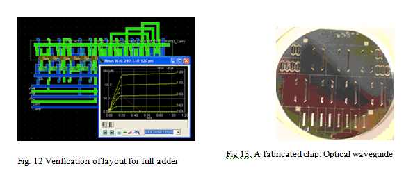
Fabrication: After verification of the extracted layout and possible correction in a very usual iterative process, the chip is sent to the foundry for fabrication. To illustrate a typical fabricated chip (the adder is too trivial for fabrication), a picture of an optical waveguide I fabricated in the Johns Hopkins University lab is shown in Fig.13. This is a clean room with high low level of impurity. Students wear hood, gloves and other covering materials to ensure that the materials being fabricated are not contaminated. It is important to point out that this lab is not state of the art, however, it has all the basic facilities that enable a complete chip fabrication. The figure shows many chips on a single die, which are subsequently cut and wire bonded. Typical steps used during the fabrication with brief explanations include:
Wafer Preparation: The wafer is the starting material. It has been produced from a very complex method called Czochralski method, which enables the production of electronically graded silicon (EGS). The EGS is very pure with 99.9999% purity level to ensure that no defect or impurity whatsoever exists that could potentially damage the fabricated systems. It is important to point out that the input to this process is special sand, silica, which after processing gives the wafer. The wafers were purchased and not processed in the lab.
Wafer Oxidation: This involves the deposition of thin layer of silicon dioxide on the wafer by exposing it to a high purity oxygen and hydrogen at high temperature. This oxide helps to form an insulation layer when the transistors gates and other components are formed.
Photoresist Coating: In this method, a light sensitive polymer was applied on the wafer while the wafer is placed on a spinner. The material, initially soluble in organic solvent, has the capacity to react with ultra-violet (uv) light and after cross-linking of the polymer bond could become insoluble. This is called a negative photoresist. There is another type of photoresist (positive photoresist) that is be initially insoluble but becomes soluble after exposure to UV light.
Exposure to UV light: The wafer covered with photoresist is exposed to uv light in a special equipment that enables the transfer of the patterns created in mask to the wafer, the silicon material. The mask is opaque in the regions that are processed and transparent in others for the negative photoresist process. Usually, during exposure, students are not allowed to watch the light since it could be harmful to the eyes.
Development and baking: The wafer in acidic solution (basic solution could be used) is developed to remove the non-exposed areas of the photoresist. Afterwards, the wafer is baked at a low temperature to harden the remaining photoresist.
Etching: This involves the selective removal of materials from areas not covered by photoresist. This is a greatly chemical process where acids, bases and others are used. It is also one of the most critical stages for a student learner. Some of these acids are dangerous and could destroy skin layers. Caution is very important at this stage.
Ion implantation: It is a means for adding dopants (impurities) to a semiconductor material (the wafer). The ions are charged and accelerated in a high electric field into the semiconductor material. An alternative process is called diffusion. However, the ion implantation is more precise and accurate than diffusion. It was done in special equipment that enabled calculated dose of the materials to be deposited at specific sections of the wafer. (There are other stages like SU-8 deposition, formation of mirror peculiar to the optical waveguide, which are not very popular. According, I will not discuss them here).
Testing: Testing is the final stage in the design flow. It involves setting a test bench to measure the electrical and electronic parameters of the chip. The test bench varies by design, as different chips would need different test methods. It is the function of the designer to design a good testing strategy for the chip. A test-setup of my optical waveguide is shown in Fig. 14. It consists of a light source, a chopper that couples the light via a lens into an optical fiber into the chip (optical waveguide). Through the aid of a photodiode the output signal from the chip is observed on an oscilloscope. From the results on the oscilloscope, I determine if the design has worked or not based on design specifications.

Conclusion: The development of highly efficient and effective entertainment hardware has been fuelled by the enormous advancement in the semiconductor industry. With continuous efforts of chip designers to develop innovative techniques to make chips smaller, robust and cheaper, gamers would continue to enjoy thrilling entertainment experience. Understanding this crucial aspect of hardware development could be intriguing for all stakeholders in the entertainment technology, especially those that use these chips to control different functions ranging from vision to automatic control. In simple general ways, the processes involved in making digital chips have been presented in this discussion.
References:
1 Etienne Sicard and Sonia D. Bendhia, Basics of CMOS Design, Tata McGraw-Hill, New Delhi, 2005
2 Yaun Taur and Edward Nowark, “CMOS devices below 0.1um: How High Will Performance Go?”, Electron Devices Meeting, Technical Digest., International Publication, pp. 215-218, 7-10 Dec 1997
3 Jan M. Rabaey, Anantha Chandrakasan, Borivoje Nikolic, Digital Integrated Circuits, 2nd edition, New Delhi, India: Pearson, 2003
4 Alain Martin, “A Program Transformation Approach to Asynchronous VLSI Design”, design. In Manfred Broy, editor, Deductive Program Design, NATO ASI. Springer, 1996
5 Scott Hauck, “Asynchronous Design Methodologies: An Overview”, Proceedings of IEEE, Vol. 83, No. 1, pp 69- 93, January 1995
6 John Uyemura, Chip Design for Submicron VLSI: CMOS layout and Simulation, Toronto: Thomson, 2006.
Note: This was written when I was a 2nd year PhD student in the Johns Hopkins University. I am sharing it, unedited and “un-updated”, to help some African students who have asked me questions on ICs and the process flow. The Association for Computing Machinery (ACM) asked me to write this for the student magazine that had a series theme on “entertainment”.


