DD
MM
YYYY

PAGES

DD
MM
YYYY

spot_img

PAGES

Home Blog Page 7487

A Reexamination: Can Venture Capitalists be Value Investors?

0

Let’s begin with some disclaimers. I have never actually been a value investor. I have also never made individual picks of stocks traded on the public markets. I was completely oblivious of stock markets until soon after I had graduated college in 2001. Before I arrived in the United States in 1997, I would not have been able to answer the question; What is a stock? During my 4 years of college I stayed narrowly focused on mathematics and physics, in which I completed a double major.

It was not till I began my professional career as an actuarial analyst at Watson Wyatt that I began to read the Wall Street Journal, and also to pay attention to news about the economy and the financial markets. I bought and read a copy of Roger Lowenstein’s Buffett: the Making of an American Capitalist. I bought the book because what I had read about value investing in the popular press at that time seemed made me think it was an investment philosophy that would agree with my temperament.

In business school at New York University’s Stern School of Business, I decided that I should petition the committee on academic standing to let me pursue an independent study on value investing. I drafted the petition, drew up a syllabus, won approval from the school, and then persuaded a professor to act as my course supervisor. My goal for the course was to learn enough about value investing to allow me to apply its precepts in what I hoped would be a career as a buy-side equity investment research analyst, studying publicly traded companies. That was 2008. Things did not work quite as I expected. I did not land at what one would traditionally think of as a securities analysis outfit. Honestly, for a while I did not know if I would land anywhere.

Eventually, I did land somewhere. Initially, my job required me to focus on helping two small companies navigate the treacherous economic climate that was the reality in 2008, 2009 and 2010. For two years that was all I did. Eventually, my responsibilities at work evolved. Now, I primarily spend my time assessing early stage technology-enabled startups for investment consideration by a venture capital fund that makes seed, series A and series B investments.

As you might expect, the shift in my responsibilities has led me back to thinking about value investing. I have asked myself what role it plays in my work. I have also been thinking about how I might apply its main precepts to my work.1

Jeffrey Bussgang tackled this subject in a piece for Fortune in October 2010, coincidentally this was not too long after I had started my very first seed stage venture capital assignment.2 I was knee deep in trying to teach myself the basics of venture capital investing. I still am. I was happy that someone else had already seen the need to tackle that question, and so I read that blog post eagerly. However, I felt a sense of intellectual dissatisfaction after I was done. So I am revisiting the question he raised. I hope I do a good job of adding to the discourse that he started. For the record, I agree with Jeff Bussgang’s conclusion – in general, it is difficult for venture capitalists to apply the concepts of value investing in a straightforward way to their work. That said, I wonder if it is not possible to apply the framework to early stage venture investing, even if the details about that application differ from what one might be accustomed to seeing or doing.

To begin the discussion I will lay out some terms that have guided how I think about this question.

When I think of a startup I prefer to use Steve Blank’s definition. According to that definition:

A startup is a temporary organization in search of a scalable, repeatable, profitable business model.3

I paraphrase that definition very slightly. A startup is a temporary organization established for the purpose of finding the solution to a problem, and to search for a scalable, repeatable, profitable business model. It is important to emphasize the process of finding a solution to a problem because it is not unusual for venture capitalists to encounter startups that have developed a solution that is seeking a problem. I try to avoid such startups. Once the startup has found a scalable, repeatable, profitable business model it begins the process of transforming itself from a startup into a company.

Venture capitalists invest in early stage, high growth startups. Usually the startups that attract the attention of venture capitalists are going into business on the basis of some innovation; technology, business model, or even a completely new invention. Generally venture-backed startups are most concentrated in areas where science, technology, engineering and mathematics play a central role. Venture capitalists typically invest after the startup has already raise some capital from friends and family, and subsequently from angel investors. However, some venture capitalists have begun to invest exclusively in seed stage startups where often the only previous capital raised by the startup is that raised from the founding team’s family and friends. The venture capitalist provides capital in exchange for an equity stake in the startup. Therefore the venture capitalist earns a return when there is an exit – an acquisition by a larger company, or an initial public offering in which shares are sold to the investing public. Venture capitalists tend to speak of themselves as people who know how to build companies. The most sought after venture capitalists tout their prior entrepreneurial experience taking innovations from idea to startup to company, and ultimately to exit. They insist that experience makes them an invaluable source of advice and ideas for entrepreneurs traveling the entrepreneurial path. There is a debate in some quarters as to wether venture capitalists’ returns derive from their ability to pick securities much like is the case for investors in the public markets, or if instead it is in fact the company building activities of venture capitalists that lead to the returns that they have realized.4

For a succinct description of value investing I turn to J. Dennis Jean-Jacques;

The goal of the value investor is quite simple: To buy solid businesses at exceptional prices in order to achieve adequate after-tax returns over a long period. The mental model is as follows: Good Business + Excellent Price = Adequate Return over Time5

One of value investing’s most important concepts is the concept of a margin of safety. To emphasize its importance in value investing Benjamin Graham says ” . . . to distill the secret of sound investment into three words, we venture the motto, MARGIN OF SAFETY. This is the thread that runs through all the preceding discussion of investment policy – often explicitly, sometimes in a less direct fashion.”6 Seth Klarman is considered one of the most successful practitioners of value investing. In discussing the concept of margin of safety he says: “A margin of safety is achieved when securities are purchased at prices sufficiently below underlying value to allow for human error, bad luck, or extreme volatility in a complex, unpredictable, and rapidly changing world.”7 Generally, margin of safety is analyzed quantitatively – in terms of a discount to intrinsic value, remembering that value investors only buy when a stock’s market price is well below their estimate of its intrinsic value, under the assumption that they understand how the stock price will gradually recover until price approaches intrinsic value.

Another central concept in value investing is the concept of an economic moat. Warren Buffett is credited with coining the term “moat” in relation to investing after he recognized that the companies that yield the most profitable investments over long investment horizons typically possess one or more characteristics that give them a durable competitive advantage. Generally, economic moats are built through some combination of economies of scale, switching costs, network effects, and intangible assets. Some value investors speak of a soft moat as the competitive advantage that a company derives from a unique corporate culture. However one does the analysis, studying the presence and durability of economic moats involves performing a qualitative analysis that is aimed at understanding how competitive advantage may be developed, and maintained.

Consider this example of an early stage startup.8 An entrepreneur raised $200,000 in seed capital 3 years ago and formed a startup with his co-founder. Working with a small team of in-house developers as well as some contractors, they have a near-final product. The product they have developed is a software product delivered over the Web to the startup’s customers. They won a competitively-bid contract with 1 country office of a large multinational corporation that has operations in more than 200 countries, selling 3,500 different products. That contract earns the startup $50,000 a month. The contract is for 3 years. They are only 3 months in. The customer is already initiating discussions to increase the number of its employees that have access to the product. The customer also wants to act as a sponsor to introduce the startup’s product to the global corporate headquarters in a bid to make the startup’s product a part of the suite of software products made available to all 200+ country offices of the corporation. These talks are in the early stages. In addition to this, the startup is in advanced discussions with other large companies that could benefit greatly from its product. Use of its product would provide these companies with a conduit into markets that they have not yet been able to access due to resource constraints. The co-founders feel they can increase monthly revenues to $100,000 a month very soon after they obtain additional capital. So far it appears that the co-founders have done a remarkable job building the product and gaining customer traction. The startup is starting to reach the point where it needs to expand in order to keep up with demand for its product, and also to access other customer segments that it has not yet been able to pursue in a focused way. The startup is raising $2,000,000 in series A financing. It holds 1 issued patent, and has submitted non-provisional applications for 4 more. All 4 are in patent prosecution. The startup expects to raise a series B financing in 18 months after it closes the series A financing. It has no debt. The post-money valuation from the previous round is not outrageous.

Is it possible to apply the precepts of value investing to this scenario? I think so. However, to do so it is necessary to extend how one applies the traditional approach to value analysis. The difficulty here is that this startup confronts us with a situation in which there is no track record, and no clear sight of the future.9 Value investing was designed for mature companies with stock trading in the public markets.10 So, how might a value-oriented venture capitalist analyze this startup?

First, I am assuming that our value-oriented early stage venture capitalist is not considering investing the full $2,000,000 that the startup needs. I am assuming that the venture capitalist will invest a minimum of $750,000 and a maximum of $1,000,000. The startup already has revenues of $50,000 per month. Assuming nothing changes, that revenue stream is locked-in for 3 years. I expect that our venture capitalist will perform some customer calls in order to assess the probability that this revenue stream will be placed at risk anytime soon. Given that the startup is already in talks with that customer to expand the scope of their relationship, I would wager a guess that the probability of that $50,000 per month revenue stream deteriorating is low. I would expect the venture capitalist to focus even more attention on the probability that on-going discussions with other customers will lead to the increase in revenues that the management team has described. Assuming a 24 month investment horizon between the completion of the series A financing and the completion of the series B financing, and assuming that the new revenues do not show up for the first 6 months after the series A financing is completed:11

Total Revenues = (24)($50,000.00) + (18)($50,000.00) = $2,100,000.00

Remember our definition of a startup? One of the main sources of uncertainty that the venture capitalist faces is that the startup could run out of capital before it concludes its search for a scalable, repeatable, and profitable business model. In this case, I think our value-oriented venture capitalist can take comfort in the fact that the startup has already engaged with one customer, and is in talks with others.12 Moreover, in addition to the capital that it will raise, the startup has significant revenues coming in that will help ensure it has enough cash to complete the most important tasks that lie ahead – growing its base of customers, growing its base of users, growing its revenues, finding its product & market fit, and settling on its business model. If the management team successfully completes each one of these tasks, there’s no reason to believe that the startup will have difficulty raising a series B round at a step-up in valuation.

So, the primary questions for our value-oriented venture capitalist are these: How acute is the problem that this startup is solving for its customers? What alternatives exist today? Does the startup solve the problem in a way that is fundamentally better than the way that problem is solved by the alternatives? Do the startup’s customers think so? What is the relative value of the solution that the startup has developed? Do its customers perceive its solution as high-, medium- or low-value? Does the startup have a culture of continuously observing its customers and improving the product in such a way that the product evolves as the startup’s customers evolve? Or, does it take the approach that its product does not need to evolve?

Looking at earnings13 in order to make an assessment about margin of safety is not something new in value investing. This is the approach Christopher H. Browne applied in his analysis of American Express after the September 11 terrorist attacks on New York City. In his own words:

Investors who realized that companies of this quality are rarely this cheap and that the income stream from the credit card business offered a margin of safety have been amply rewarded in the years since.14

Second, I expect our value oriented venture capitalist to devote some time to studying the prospect that this startup can create an economic moat around itself. To do this, I think there are at least 10 areas that the venture capitalist should study.15 For each area, I rate the startup I am studying as high, medium, or low. These are the areas:

  1. Sustainable competitive advantage; why does it exist, how long is it likely to last?
  2. Network effects; why do they exist, how long are they likely to last?
  3. Revenue; how predictable is revenue, once it is secured?
  4. Switching costs; once a customer is secured, do switching costs exist?
  5. Gross profitability; is gross profitability high, medium, or low? How does gross profitability evolve as the startup grows?
  6. Marginal profitability; is marginal profitability high, medium, or low? How does marginal profitability evolve as the startup grows?
  7. Customer concentration; how profitable is each additional customer? I prefer startups that will quickly evolve to avoid falling victim to buyer power. Many small but highly profitable customers is better than a few powerful and demanding customers.
  8. Partner dependency; is the startup dependent on its partners? What is the nature of that dependency? I prefer the startup not to be so dependent on its partners that an adverse change in the relationship proves fatal for the startup. Several startups have failed after Facebook and Twitter changed the nature of the partnership relationship they had with startups that built products on top of the traffic produced by Facebook and Twitter.16
  9. Demand creation; how much will it cost the startup to create additional demand? I prefer startups that do not need to spend large amounts of money in order to create new demand. I spend a lot of my time thinking about this.
  10. Future growth; what are the prospects for future growth? Or, how big is the opportunity that is available to the startup? Bigger is always better in this case – room for more than one player to earn an attractive returns for early investors.

This line of analysis fits well conceptually with a 3-part analysis framework for value investors that is outlined by Bruce Greenwald and Judd Kahn in their book.17 The areas of analysis they highlight are asset value, earnings power value, and value of growth. For any startup asset value is none-existent, or almost nil. Allowing for variability, once the startup has found its product & market fit its ability to generate earnings should increase. Lastly, if the startup is solving an important enough problem in a big enough market, there should be enough room for future growth to earn an attractive return for our value-oriented venture capitalist.

There are numerous pitfalls to the approach I have tried to describe above. First, it is really difficult to estimate intrinsic value for an early stage startup. Second, the approach I have suggested does not change the fact that what our value oriented venture capitalist cannot possibly know far exceeds what is known in relation to the future prospects for this startup. Third, the venture capitalist must spend a considerable amount of time studying the management team of the startup in question. Building an early stage startup is an extremely daunting challenge. Much of our value-oriented venture capitalist’s ability to earn a return rests upon the management team making the right decisions at crucial periods in the startup’s life-cycle. Certain individuals, or combination of individuals, simply lack the temperament to succeed in leading an early stage startup successfully. Last, even after taking all the precautions that one can take, our value-oriented venture capitalist might still wind up making a poor investment – that is true for every value investor, but I expect the frequency of poor results to be higher for a value-oriented venture capitalist than for a traditional value investor.

I have glossed over numerous details by necessity. Fruitful implementation of a value-oriented approach to early stage venture capital investing is all about the details of each specific situation. For instance, I do not know if one can apply a value-oriented approach to startups raising capital at the seed and pre-seed stage. I think this approach only works when the startup has gained some market traction. I have not discussed how investment horizons might factor into this. I default to Warren Buffet’s view that one should invest as if one were buying an ownership stake in a company for the long-haul and not as if one is buying tradable pieces of paper.

I do not know if venture capitalists need to be able to see around corners, but I think they have to do in-depth analysis of the startups in which they invest, and I think they have to spend sometime thinking about the similarities and differences between the early stage startups that they study and the traits of the most successful public companies that were themselves early stage startups at some point in the past.

Early stage venture capitalists can apply the tenets of value investing to what they do, provided they are willing to do some extra work, and are willing to look beyond the most obvious methods that other value investors use.


  1. Any mistakes in quoting from my sources are entirely mine. ?
  2. Jeffrey Bussgang, Can VCs Be Value Investors?, Fortune, October 6, 2010. Accessed at http://finance.fortune.cnn.com/2010/10/06/can-vcs-be-value-investors/ on August 10, 2013. ?
  3. Steve Blank and Bob Dorf, The Startup Owner’s Manual Vol. 1: The Step-by-Step Guide for Building a Great Company, California, K&S Ranch Press, 2012, page xvii. ?
  4. I am greatly simplifying things for the sake of brevity, but this covers the basics. ?
  5. J. Dennis Jean-Jacques, The Five Keys To Value Investing, New York, McGraw-Hill, 2002, page 2. ?
  6. Benjamin Graham, The Intelligent Investor, New York, HarperCollins, the 2005 reprint of the original 1949 edition, page 241. ?
  7. Seth Klarman, Margin of Safety: Risk-Averse Value Investing Strategies for The Thoughtful Investor, New York, HarperCollins, 1991, page 92. ?
  8. While this specific example is entirely fictitious, it is not entirely dissimilar to many of the situations that early stage venture capitalists have to study in order to make an investment decision. ?
  9. Tobias Carlisle discusses this in a post from October 7, 2010 entitled Venture Capitalists, Value Investing and Facebook. You can find it here: http://greenbackd.com/2010/10/07/venture-capitalists-value-investing-and-facebook/ ?
  10. Value investors might be able to adapt their approach to suit mature privately held companies. ?
  11. Since this is a software startup we expect expenses to increase at only a fraction of the increase in revenues, so I will not focus too much on expenses. ?
  12. All customers are not created equal. ?
  13. I am using terms somewhat loosely here; technically revenues are not the same as earnings. ?
  14. Christopher H. Browne, The Little Book of Value Investing, New Jersey, John Wiley & Sons, 2007, page 68. ?
  15. I use a grid that I developed based on Bill Gurley’s post; All Revenue is Not Created Equal: Keys to the 10X Revenue Club. You will find that post here: http://abovethecrowd.com/2011/05/24/all-revenue-is-not-created-equal-the-keys-to-the-10x-revenue-club/ ?
  16. Alyson Shontell, An Obvious Reason Why Some Startups Fail Shortly After Raising Tons Of Money, August 8, 2013: www.sfgate.com/technology/businessinsider/article/An-Obvious-Reason-Why-Some-Startups-Fail-Shortly-4717874.php ?
  17. Bruce C. N. Greenwald and Judd Kahn, Value Investing: From Graham to Buffet and Beyond, New Jersey, John Wiley & Sons, paperback edition, 2001, page 35 – 47. ?

Shiva Ayyadurai files a $15M suit as “inventor of email” against a website for questioning his accomplishments

0

We all use email but it seems finding the original creator is not going to be cheap.

TechDirt broke his silence on Wednesday about a $15 million lawsuit filed by the self-proclaimed “inventor of email,” Shiva Ayyadurai, who is suing the site for questioning his accomplishments.

Tech Dirt has noted that it stands by its claims that email existed long before Ayyadurai wrote an email-related software program, and said the site would fight the lawsuit as baseless.

As you may have heard, last week we were sued for $15 million by Shiva Ayyadurai, who claims to have invented email. We have written, at great length, about his claims and our opinion — backed up by detailed and thorough evidence — that email existed long before Ayyadurai created any software. We believe the legal claims in the lawsuit are meritless, and we intend to fight them and to win.

There is a larger point here. Defamation claims like this can force independent media companies to capitulate and shut down due to mounting legal costs. Ayyadurai’s attorney, Charles Harder, has already shown that this model can lead to exactly that result. His efforts helped put a much larger and much more well-resourced company than Techdirt completely out of business.

Very interesting that someone can be offended that way to ask for $15 million.

What makes a company a Digital Leader?

0

A survey of 573 global companies reveals that just 13% of them have integrated digital technologies enterprise-wide, which resulted in improved efficiency, customer experience, and business models.

These are the leaders of digital transformation and what they do:

  • Focus on growth: 63% say revenue and margin growth is the top measure of success
  • Invest more in digital transformation:  51% plan to dedicate 10% or more of revenues to digital transformation over the next two years
  • Excel at Customer Experience: 40% are creating new markets thanks to digital transformation
  • More advanced in Data Analytics: 43% have data and analytics integrated at the enterprise level
  • Reap more benefits from data and analytics: 40% have increased revenue from data & analytics by 5% or more

Source: Forbes Insights Print

How to Design and Make Integrated Circuits

0

Introduction

Most modern entertainment gadgets, equipment and tools incorporate integrated circuits that perform some specific functions that make the entertainment experience fascinating for users. From the simple toys for toddlers to the complex game studios in casinos, hardware forms a major component of entertainment technology. With the advent of integrated circuits, and subsequent development of CMOS (complementary oxide semiconductor) technologies, there has been remarkable success in the number of application specific integrated chips (ASIC) tailored for gaming and general entertainment. And from programmable micro-controllers to field programmable gate arrays (FPGAs), chips are common tools to both computer scientist and engineer. Consequently, understanding the fascinating processes used in making these chips which are programmed and used in circuit boards could be interesting for all stakeholders in the field of entertainment technology. The design of integrated circuit is perhaps one of the most complex stages in the development process of game and entertainment infrastructure forming a vital part of the entertainment technology. Increasingly, chip designers are discovering ways of implementing functions hitherto done with massive codes of computer programs inside integrated circuits.

Integrated circuits are circuits that could contain millions of transistors and other circuit elements on a single die (a piece of silicon that contains active devices and input and output interfaces) [1]. They are made on special materials called semiconductors with silicon and gallium arsenide (GaAs) the most common.  Its evolution is a major milestone in the history of modern industry as it has driven a revolution in computing capability due to a long trend in performance, density gains, and cost with scaling [1,2]. Remarkably, these circuits could be made using different technologies. But over time, complementary metal oxide semiconductor (CMOS) technology has become the industry de-facto and the most prevalent method of choice. Its major advantages over other technologies are its ease of integration of circuit components and low static power consumption [3]. This is the main technology used to make analog-to-digital converters, micro-controllers, FPGA (an integrated circuit that contains an array of identical cells with programmable interconnections), microprocessors and host of others that are used while developing entertainment hardware. Its continuous improvements has driven reduction in size of game gadgets, better performance, more efficient battery management for battery operated devices, cost as well as hardware ergonomics.

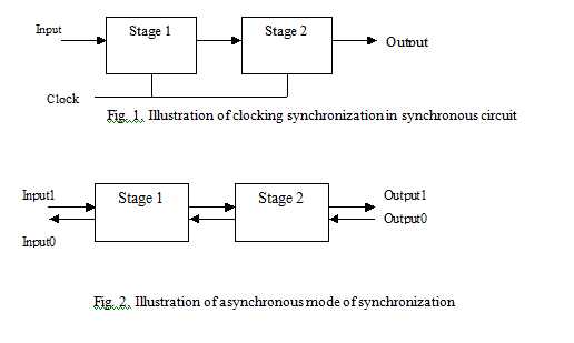
Integrated circuit could be digital, analog or mixed signal (a combination of both analog and digital). While the digital chip involves designing at logic levels of 1 and 0, the analog is based on continuous signal. Besides, sequencing and communication synchronization on chip could be done by use of globally distributed clocks for synchronous designs or local handshaking variables for asynchronous designs.  Between these two methods, the former is the more common method. However, issues like switching delay, complexity management and clock distributions, which may place limitation on synchronous chip performance with an acceptable level of reliability as technology is scaled down, had stimulated interests in the study of asynchronous systems [4,5]. Asynchronous chips are known as self timed circuits since they do not use clocks but rather use local variables that perform the functions of handshaking requests and acknowledgements. Design of asynchronous digital system involves an entirely different concept when compared to synchronous design. The idea of clockless system introduces so many design parameters, which must be tracked as the requests, and acknowledgements signals are generated and routed. The initial stage of asynchronous system development would interest a computer scientist because of enormous digital “coding” that describes level of system abstraction.

For an illustration of the two design techniques, consider Fig. 1 where a signal, clock, is used to coordinate the functional operations of the circuit. The clock signal enables the circuit to manage the beginning of an operation, its termination and the beginning of another one and so on. Correct functionality of this circuit partly depends on the clock and any problem with this signal could potentially affect the accuracy of the functions being performed. On the other hand, consider Fig.2 where there is no clock signal. Rather, local signals, called handshake signals (actually request and acknowledgement signals), are used to coordinate when an operation has started, terminated and so forth. The implication is that subsequent operations must wait until the proceeding ones have started and completed based on design without regard to any global control signal. However, this usually comes at the expense of more wiring. For this article, I will focus on the synchronous system due to its popularity.

Integrated Circuit Design Flow

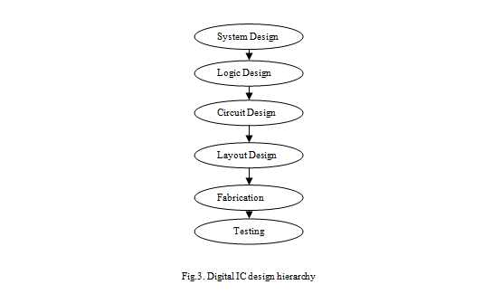
The process of chip design is very complex and its understating requires many years of study and practical experience. From a digital integrated circuit design perspective, it could be divided into different hierarchies as shown in Fig.3 where the problems are examined at several different levels [6].

System Design:  This stage provides the specifications and main operations of the chip. It examines such issues like chip area, power, functionality, speed, cost and other design factors while setting these specifications. Sometimes, the resources available to the designer could act as a constraint during this stage. For instance, a designer may like to design a chip to work at 1.2V, but available process technology can only support a voltage of 5V. In this situation, the designer has to adjust these specifications to satisfy the available tools. It is always a good habit to understand the process technology available before system design and specifications. Process technology is basically the specific foundry technology rules where the chip would be fabricated. Typical examples are AMI 0.5um, TSMC 0.35um and IBM 0.13um. A design based on one process technology is unique to that process and accordingly should be fabricated in a foundry that supports that process. At the system design level, the main sections of the system are illustrated with block diagrams, with no details on the contents of the blocks. Only the input and output characteristics of the sections are detailed [6].

Logic Design: At this stage, the designer implements the logic networks that would realize the input and output characteristics specified in the previous stage.  This is generally made of logic gates with interconnecting wires that are used to realize the design.

Circuit Design: Circuit design involves the translation of the various logic networks into electronic circuitries using transistors. These transistors are switching devices whose combinations are used to realize different logic functions. The design is tested using computer aided design (CAD) tools and comparisons are made between the results and the chip specifications.  Through these results, the designer could have an idea of the speed, power dissipation, and performance of the final chip. An idea of the size of the chip is also obtained at this stage since the number of transistors would determine the area of the chip. Experienced designers optimize many design variables like transistor sizes, transistor numbers, and circuit architecture to reduce delay, power consumption, and latency among others. The length and width of the transistors must obey the rules of the process technology.

Layout Design: This stage involves the translation of the circuit realized in the previous stage into silicon description through geometrical patterns aided by CAD tools [3,6]. This translation process follows a process rule that specifies the spacing between transistors, wire, wire contacts and so on. Violation of these rules results to malfunctioning chips after fabrication.  Besides, the designer must ensure that the layout design accurately represents the circuit design and that the design is free of errors. CAD tools enable checks for errors and also incorporate ways of comparing layout and circuit designs provided in form of Layout Versus Schematic (LVS) checks. When errors are reported, the designer has to effect the corrections.  A vital fundamental stage in layout design is Extraction, which involves the extraction of the circuit schematic from the layout drawings.  The extracted circuit provides information on the circuit elements, wires, parasitic resistance and capacitance (a parasitic device is an unbudgeted device that inserts itself due to interaction between nearby components). With the aid of this extracted file, the electronic behavior of the silicon circuit is simulated and it is always a good habit to compare the results with the system specification since this is one of the final design stages before a chip is sent to the foundry.

Fabrication: Upon satisfactory verification of the design, the layout is sent to the foundry where it is fabricated. The process of chip fabrication is very complex. It involves many stages of oxidation, etching, photolithography, etc. Typically, the fabrication process translates the layout into silicon or any other semiconductor material that is used. The result is bonded with pins for external connections to circuit boards.

Fabrication process uses photolithographic masks, which define specific patterns that are transferred to silicon wafers (the initial substrate used to fabricate integrated circuits) through a number of steps based on the process technology. The starting material, the wafer, is oxidized to create insulation layer in the process. It is followed by photolithographic process, which involves deposition of photoresist on the oxidized wafer, exposure to ultra-violet rays to form patterns and etching for removal of materials not covered by photoresist. Ion implantation of the p+ or n+ source/drain region and metallization to form contacts follow afterwards. The next stage is cutting the individual chip from the die. For external pin connection, bonding is done. It is important to emphasize that this process steps could be altered in any order to achieve specific goals in the design process. In addition, many of these functions are done many times for very complex chips. Over the years, other methods have emerged. A notable one is the use of insulators (like sapphire) as starting materials instead of semiconductor substrate (the silicon on which active devices are implanted) to build the transistors. This method called Silicon on Insulator (SOI) minimizes parasitic in circuits and enable the realization of high speed and low power dissipation chips [6].

Testing: The final stage of the chip development is called testing. Electronic equipment like oscilloscopes, probes, pattern generators and logic analyzers are used to measure some parameters of the chip to verify its functionalities based on the stated specifications. It is always a good habit to test for various input patterns for a fairly long time in order to discover possible performance degradation, variability, or failures. Sometimes, fabricated chip test results deviate from simulated results. When that occurs, depending on application, the designer could re-engineer the circuit for improvement and error corrections. The new design should be fabricated and tested at the end.


A Case study

For simplicity, let us imagine the design of a simple chip that would enable an addition of player’s score during a video game. One vital component of that chip would be an arithmetic logic unit (ALU). Many ALU have adder circuits inside. We would use the design of a simple full adder to illustrate the design process discussed above. This is a trivial design and in no way a representative of the level of work in state of the art digital circuits used in computers, games, etc.

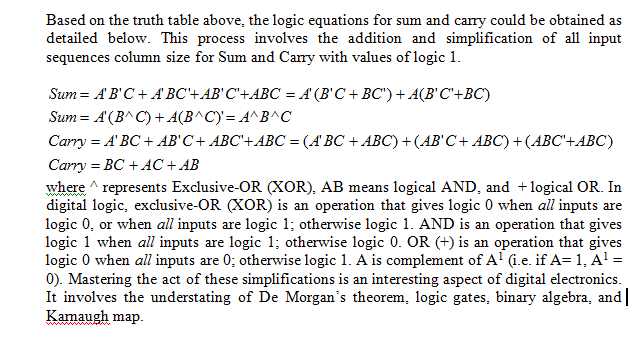
System Design: The truth table of a full adder is presented in Table 1. There are two digital inputs and a carry-in bit. The sum and carry are the results of the adder based on the sequence of inputs. The implementation is on CMOS 0.6um (minimum transistor length of 0.6 micrometer) and the voltage levels are 5V(Vdd) and 0V(GND). In digital logic, these are represented as 1 (high voltage) and 0 (low voltage) respectively. We could specify the maximum power dissipation and speed if the design is very complex at this stage. Sum and Carry are obtained by digital addition of the input sequences as represented in the truthtable, a combination table that specifies the values of Boolean expression for all possible input sequences. Ability to build truthtable is very important in digital design since it enables the designer to evaluate all the input sequences with output results. It is a prerequisite to successful design of digital systems. For instance, when A=B=C=1, the addition of 1+1+1 = 3. Converting 3 to binary (base two) is 11. So we represent the Sum as 1 and Carry as 1. For input sequence of A=B=1 and C=0, the addition 1+1+0 =2 and converting 2 to base two gives 10. Hence, Sum takes 0 and Carry 1.

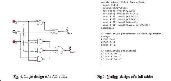
Logic Design: The logic implementation of the adder is given in Fig.4. This is the top-level entity with instantiated components of exclusive-OR (XOR), 2-input and 3-inputs NAND gates. Each of these components must be verified and tested as standalone before they can be used in the top-level. As shown in the figure, input sequence (A=1, B=0, C=1) will result to Sum =0, and Carry =1.

Alternatively, the logic design could be done with the aid of high-level description language such as VHDL (VHSIC Hardware Description Language, with VHSIC standing for Very High Speed Integrated Circuit) or Verilog. This offers a way of managing complexity associated with high performance systems on chip (SOC) as well as aid testing and verification of design before implementation in hardware. This is a smart strategy since it would be inconceivably impossible to implement state of the art microprocessor with millions of transistors using logic design. Such a method would be cumbersome, time consuming, ineffective and failure prone since it would be difficult for the designer to keep tracks of the design. For this reason, ability to “code” in VHDL or Verilog is a major skill required for all digital designers. Using these languages, a digital system is described in a textual format based on syntax used to specify gates and wires. It also offers specific delay information and hardware specific parameters that make design validation a lot easier.  This design could be a structural, or behavioral description of the design. A Verilog design of the full adder is presented in Fig.5.

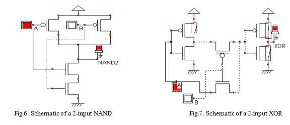
Circuit Design: The design of the full adder as noted above involves XOR and NAND gates. The circuit design would implement these designs in form of schematics using transistors. Understanding the behaviors of transistors, both the PMOS and NMOS is vital to designing and realizing these logic gates. The schematic design of 2-input NAND and XOR are presented in Fig.6 and Fig.7 respectively. To test these circuits, input sequences (A= 1, B=0) are applied to the circuits. The results shown are accurate based on the behavior of NAND and XOR gates. For NAND, input sequence of A=B=1 gives 0, while others input sequences return 1. NAND is a complement of AND, or in other words, an inverted AND (logic 1 is complement of logic 0 and vice versa). For XOR, input sequences (A=B =1; A=B=0) return 0 while others give 1. For the full adder, the complete schematics would incorporate all the schematics of the logic gates. Sizing of the transistors used in the design is very crucial as it does affect circuit performance.

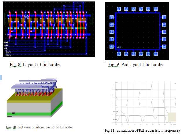
Layout Design: The full adder is translated into a silicon description based on design rule specified by the CMOS 0.6um rule. Basically, every wire, transistor, contact or any section of the circuit could be represented by polygons of different materials. It could be metal for connection, poly (special type of silicon) for making transistors or via for contacts among others. The length and width of these polygons designate the sizes of circuit elements they represent. Fig. 8 shows a 2-D layout of the design, which is made up of many different layers, each represented by a different color.  The blue sections represent different metal layers, while the red sections are a special type of silicon called poly-silicon. When a poly-silicon crosses a Select (a diffusion region), transistor is formed. The PMOS transistors are enclosed in a N-well since the starting substrate of the design is a p-substrate.  Usually, many CAD tools have facilities that check for errors in the design based on the process technology. Any violation of the rule must be corrected in the layout. In an analog design, layout is more complex because of problems of parasitic and crosstalks (kind of interference in the system). Consequently, analog layout must be protected and shielded from sources of noise.  Pad frame layout that provides input/output ports to the chip is shown in Fig. 9. The pads are stack of metal squares connected by contacts that surround the central core region with signal assignments for easy wiring access to the circuits. A better view of this layout is shown in a 3-D as shown in Fig.10. The figure shows the different layers of diffusion, oxide, etc that have been carried out  to realize the circuit.

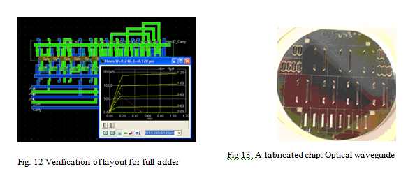
The verification of the layout is very important and crucial. After extraction of the layout, the result is simulated to check correctness in design. There are many ways this could be done depending on the nature of the design. It could be by checking the current, voltage levels and other circuit parameters for correctness. Fig. 11 is a simulation of the adder, which has a problem of slow response time and consequently degraded performance. The problem has come from the sizing of the transistors during the circuit level. This is subsequently corrected. Knowing that any uncorrected error would reflect in the fabricated chip calls for detailed attention at this stage. Fig. 12 shows a simulation process verifying some circuit parameters for the full adder.

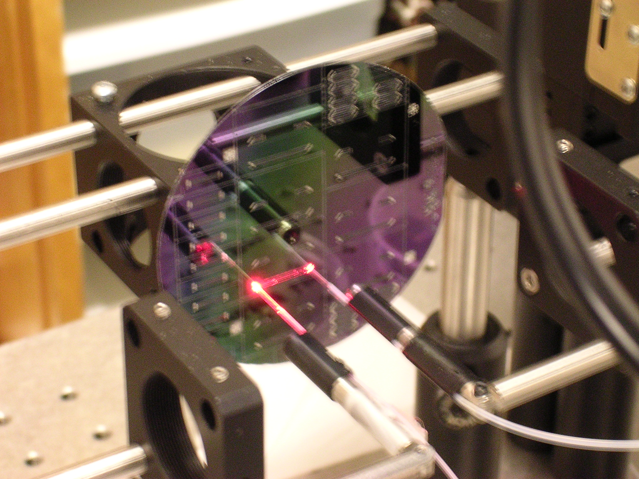
Fabrication: After verification of the extracted layout and possible correction in a very usual iterative process, the chip is sent to the foundry for fabrication. To illustrate a typical fabricated chip (the adder is too trivial for fabrication), a picture of an optical waveguide I fabricated in the Johns Hopkins University lab is shown in Fig.13. This is a clean room with high low level of impurity. Students wear hood, gloves and other covering materials to ensure that the materials being fabricated are not contaminated.  It is important to point out that this lab is not state of the art, however, it has all the basic facilities that enable a complete chip fabrication. The figure shows many chips on a single die, which are subsequently cut and wire bonded. Typical steps used during the fabrication with brief explanations include:

Wafer Preparation: The wafer is the starting material. It has been produced from a very complex method called Czochralski method, which enables the production of electronically graded silicon (EGS). The EGS is very pure with 99.9999% purity level to ensure that no defect or impurity whatsoever exists that could potentially damage the fabricated systems. It is important to point out that the input to this process is special sand, silica, which after processing gives the wafer. The wafers were purchased and not processed in the lab.

Wafer Oxidation: This involves the deposition of thin layer of silicon dioxide on the wafer by exposing it to a high purity oxygen and hydrogen at high temperature. This oxide helps to form an insulation layer when the transistors gates and other components are formed.

Photoresist Coating: In this method, a light sensitive polymer was applied on the wafer while the wafer is placed on a spinner. The material, initially soluble in organic solvent, has the capacity to react with ultra-violet (uv) light and after cross-linking of the polymer bond could become insoluble. This is called a negative photoresist. There is another type of photoresist (positive photoresist)  that is be initially insoluble  but becomes soluble after exposure to UV light.

Exposure to UV light: The wafer covered with photoresist is exposed to uv light in a special equipment that enables the transfer of the patterns created in mask to the wafer, the silicon material. The mask is opaque in the regions that are processed and transparent in others for the negative photoresist process. Usually, during exposure, students are not allowed to watch the light since it could be harmful to the eyes.

Development and baking: The wafer in acidic solution (basic solution could be used) is developed to remove the non-exposed areas of the photoresist. Afterwards, the wafer is baked at a low temperature to harden the remaining photoresist.

Etching:  This involves the selective removal of materials from areas not covered by photoresist. This is a greatly chemical process where acids, bases and others are used. It is also one of the most critical stages for a student learner. Some of these acids are dangerous and could destroy skin layers. Caution is very important at this stage.

Ion implantation:  It is a means for adding dopants (impurities) to a semiconductor material (the wafer). The ions are charged and accelerated in a high electric field into the semiconductor material. An alternative process is called diffusion. However, the ion implantation is more precise and accurate than diffusion. It was done in special equipment that enabled calculated dose of the materials to be deposited at specific sections of the wafer. (There are other stages like SU-8 deposition, formation of mirror peculiar to the optical waveguide, which are not very popular. According, I will not discuss them here).

Testing: Testing is the final stage in the design flow. It involves setting a test bench to measure the electrical and electronic parameters of the chip.  The test bench varies by design, as different chips would need different test methods. It is the function of the designer to design a good testing strategy for the chip. A test-setup of my optical waveguide is shown in Fig. 14. It consists of a light source, a chopper that couples the light via a lens into an optical fiber into the chip (optical waveguide). Through the aid of a photodiode the output signal from the chip is observed on an oscilloscope. From the results on the oscilloscope, I determine if the design has worked or not based on design specifications.

Conclusion: The development of highly efficient and effective entertainment hardware has been fuelled by the enormous advancement in the semiconductor industry. With continuous efforts of chip designers to develop innovative techniques to make chips smaller, robust and cheaper, gamers would continue to enjoy thrilling entertainment experience. Understanding this crucial aspect of hardware development could be intriguing for all stakeholders in the entertainment technology, especially those that use these chips to control different functions ranging from vision to automatic control. In simple general ways, the processes involved in making digital chips have been presented in this discussion.


References:

1          Etienne Sicard and Sonia D. Bendhia, Basics of CMOS Design, Tata McGraw-Hill, New Delhi, 2005

2          Yaun Taur and Edward Nowark,  “CMOS devices below 0.1um: How High Will Performance Go?”, Electron Devices Meeting, Technical Digest., International  Publication, pp. 215-218, 7-10 Dec 1997

3          Jan M. Rabaey, Anantha Chandrakasan, Borivoje Nikolic, Digital Integrated Circuits, 2nd edition, New Delhi, India: Pearson, 2003

4          Alain Martin, “A Program Transformation Approach to Asynchronous VLSI Design”, design. In Manfred Broy, editor, Deductive Program Design, NATO ASI. Springer, 1996

5          Scott Hauck, “Asynchronous Design Methodologies: An Overview”, Proceedings of IEEE, Vol. 83, No. 1, pp 69- 93, January 1995

6          John Uyemura, Chip Design for Submicron VLSI: CMOS layout and Simulation, Toronto: Thomson, 2006.


Note: This was written when I was a 2nd year PhD student in the Johns Hopkins University. I am sharing it, unedited and “un-updated”, to help some African students who have asked me questions on ICs and the process flow. The Association for Computing Machinery (ACM) asked me to write this for the student magazine that had a series theme on “entertainment”. 

Apply to demo your product in New York Stock Exchange at the Kairos Global Summit in April 2017

0

Kairos 50 is looking for the 50 of the world’s most innovative companies founded by the next generation of entrepreneurs. This year’s K50 class will demo on the trading floor of the New York Stock Exchange at the Kairos Global Summit on April 21-22, 2017

Who qualifies for the K50?

Each K50 Applicant must meet the following criteria:

  • Co-Founder Status: the applicant/nominee must be a co-founder of the company.
  • Age Eligibility: he or she must have been under the age of 26 at the time the company was founded.
  • Working Product/Prototype: each company must have a product or prototype that can be demoed at the time of submission.
  • Business Model: must clearly fit one of the following two categories:
    • Cutting-edge Technologies Entering Massive, Outdated Industries (such as transportation, logistics, healthcare)
    • New Products & Services Addressing Fundamental Human Needs
  • Kairos Global Summit Attendance: he or she must be able to attend and showcase the product or prototype at the Kairos Global Summit, which takes place in New York, NY from April 21-22. They may bring other co-founders or team members.
  • Fundraising: companies should be pre Series A at the time of application.
  • References: applicants must have at least one reference to give feedback to Kairos on their team, product, and traction.

Qualified? Apply here