DD
MM
YYYY

PAGES

DD
MM
YYYY

spot_img

PAGES

Home Blog Page 7937

‘Entrepreneurial Solutions’ Transform BoP Markets for Prosperity

0

The quest for prosperity requires a radical shift in perspective. This book will equip entrepreneurs and other leaders with a roadmap for success.

New York, NY – Four billion people – more than half of the world’s population – lives on less than $2/day. A revolution is underway where these citizens refuse to be stuck in survival. Recent events in Egypt illustrate this cry for change.

Yet, leading business thinkers have identified this population – often called the “Base of the Pyramid” (BoP) – as one of the greatest opportunities of the 21st century.

Many business leaders have considered these markets “too difficult to crack” – or have failed trying to do so. Similarly, entrepreneurs operating in Base of the Pyramid markets struggle to realize the economic potential of the market.

Author Eric Kacou identifies the problem as the ‘survival trap’ a tendency for businesses and nations to focus on short-term crises at the expense of developing long-term strategies for prosperity.  This vicious cycle keeps individuals poor, businesses struggling, and nations under-developed.

This book is about prosperity creation in business and society.” states Kacou about his new book, Entrepreneurial Solutions for Prosperity in BoP Markets (Wharton School Publishing, ISBN-13: 9780137079261, 336 pages, $29.99, January 2011). After identifying outdated mindsets which have lead to mistrust, dependence, and failure, this book shares the secrets of entrepreneurs that have made it and are transforming the Base of the Pyramid markets where they operate.

What do the successes of these entrepreneurs and of nations like Rwanda teach us about fostering the entrepreneurial spirit at the Base of the Pyramid?  What practical techniques can business and government leaders use to unleash the untapped potential of this huge market?

Kacou identifies the breakthrough mindsets, business models and operational techniques for success. Drawing from research and experience in low-income nations, Kacou reveals seven opportunities for unleashing a virtuous cycle of prosperity. These seven opportunities equip readers with the tools to take their economic destiny in their own hands.

Rather than a call for outside help, Entrepreneurial Solutions for Prosperity in BoP Markets is a call to action for entrepreneurs and other leaders. It equips citizens at the BoP with the tools necessary to take control of their economic destiny. Specifically, readers will gain a better understanding of:

  • Why Mindsets Matter: mindsets drive actions and by extension results at base of the pyramid. Stakeholders have the power to improve their reality by adopting new mindsets. This book offers specific mindsets that can act as keys to escape the Survival Trap.
  • What are the Solutions for Escaping the Survival Trap: after offering a diagnostic tool of prevailing mindsets, this book proposes human-centric approaches for prosperity.  Rooted in the reality of BoP markets, these seven approaches align businesses to the specific challenges of operating in low-income nations.
  • How to deploy these solutions for business success and economic transformation: integration is required to move from individual success to broad based prosperity. Rwanda’s metamorphosis provides the capstone example of the power of collectively embracing entrepreneurial mindsets.

At a time of transformative choices, discerning leaders now have a blueprint for prosperity. By unleashing an entrepreneurial revolution, the energies of half of the world’s population will be leveraged as the base of the pyramid lifts itself out of poverty.

Check out an excerpt from the book by visiting www.entrepreneurialsolutionsforprosperity.com

If you are interested in receiving a copy of Entrepreneurial Solutions for Prosperity in BoP Markets (electronic format also available) or an interview with the author, please contact Charity Kabango at 647-833-7496 / ckabango@entrepreneurialsolutionsforprosperity.com

About the Author

A native of Cote d’Ivoire, Eric Kacou is co-founder and CEO of Entrepreneurial Solutions Partners (ESP), a firm providing entrepreneurs and leaders with the right mix of insight and capital needed to generate prosperity. Prior to starting this venture, this, he served as Managing Director of OTF Group, a competitiveness consultancy focused on emerging markets. An expert in business strategy and economic reconstruction, he led the Rwanda National Innovation and Competitiveness (RNIC) Program. Eric also served CEOs and leaders of over a dozen developing countries and international development partners. Eric started his career as a strategy consultant with Monitor Company advising Fortune 500 executives. A candidate Mason Fellowship in Public Policy at the Harvard Kennedy School, Eric earned his MBA at the Wharton School, and serves on the Wharton Executive Board for Europe, Africa and the Middle East. The World Economic Forum honored Eric Kacou as a Young Global Leader.

Integrated Circuit Design Flow

0

The process of chip design is very complex and its understating requires many years of study and practical experience. From a digital integrated circuit design perspective, it could be divided into different hierarchies or stages where the problems are examined at several different levels: system design, logic design, circuit design, layout design, fabrication and testing. These steps are not necessarily sequential; interactions are done in practice to get things right.

System Design: This stage provides the specifications and main operations of the chip. It examines such issues like chip area, power, functionality, speed, cost and other design factors while setting these specifications. Sometimes, the resources available to the designer could act as a constraint during this stage. For instance, a designer may like to design a chip to work at 1.2V, but available process technology can only support a voltage of 5V. In this situation, the designer has to adjust these specifications to satisfy the available tools. It is always a good habit to understand the process technology available before system design and specifications. Process technology is basically the specific foundry technology rules where the chip would be fabricated. Typical examples are AMI 0.5um, TSMC 0.35um and IBM 0.13um. A design based on one process technology is unique to that process and accordingly should be fabricated in a foundry that supports that process. At the system design level, the main sections of the system are illustrated with block diagrams, with no details on the contents of the blocks. Only the input and output characteristics of the sections are detailed.

Logic Design: At this stage, the designer implements the logic networks that would realize the input and output characteristics specified in the previous stage. This is generally made of logic gates with interconnecting wires that are used to realize the design.

Circuit Design: Circuit design involves the translation of the various logic networks into electronic circuitries using transistors. These transistors are switching devices whose combinations are used to realize different logic functions. The design is tested using computer aided design (CAD) tools and comparisons are made between the results and the chip specifications. Through these results, the designer could have an idea of the speed, power dissipation, and performance of the final chip. An idea of the size of the chip is also obtained at this stage since the number of transistors would determine the area of the chip. Experienced designers optimize many design variables like transistor sizes, transistor numbers, and circuit architecture to reduce delay, power consumption, and latency among others. The length and width of the transistors must obey the rules of the process technology.

Layout Design: This stage involves the translation of the circuit realized in the previous stage into silicon description through geometrical patterns aided by CAD tools. This translation process follows a process rule that specifies the spacing between transistors, wire, wire contacts, and so on. Violation of these rules results to malfunctioning chips after fabrication. Besides, the designer must ensure that the layout design accurately represents the circuit design and that the design is free of errors. CAD tools enable checks for errors and also incorporate ways of comparing layout and circuit designs provided in form of Layout Versus Schematic (LVS) checks. When errors are reported, the designer has to effect the corrections. A vital fundamental stage in layout design is Extraction, which involves the extraction of the circuit schematic from the layout drawings. The extracted circuit provides information on the circuit elements, wires, parasitic resistance and capacitance (a parasitic device is an unbudgeted device that inserts itself due to interaction between nearby components). With the aid of this extracted file, the electronic behavior of the silicon circuit is simulated and it is always a good habit to compare the results with the system specification since this is one of the final design stages before a chip is sent to the foundry.

Fabrication: Upon satisfactory verification of the design, the layout is sent to the foundry where it is fabricated. The process of chip fabrication is very complex. It involves many stages of oxidation, etching, photolithography, etc. Typically, the fabrication process translates the layout into silicon or any other semiconductor material that is used. The result is bonded with pins for external connections to circuit boards.

Fabrication process uses photolithographic masks, which define specific patterns that are transferred to silicon wafers (the initial substrate used to fabricate integrated circuits) through a number of steps based on the process technology. The starting material, the wafer, is oxidized to create insulation layer in the process. It is followed by photolithographic process, which involves deposition of photoresist on the oxidized wafer, exposure to ultra-violet rays to form patterns and etching for removal of materials not covered by photoresist. Ion implantation of the p+ or n+ source/drain region and metallization to form contacts follow afterwards. The next stage is cutting the individual chip from the die. For external pin connection, bonding is done. It is important to emphasize that this process steps could be altered in any order to achieve specific goals in the design process. In addition, many of these functions are done many times for very complex chips. Over the years, other methods have emerged. A notable one is the use of insulators (like sapphire) as starting materials instead of semiconductor substrate (the silicon on which active devices are implanted) to build the transistors. This method called Silicon on Insulator (SOI) minimizes parasitic in circuits and enable the realization of high speed and low power dissipation chips.

Testing: The final stage of the chip development is called testing. Electronic equipment like oscilloscopes, probes, pattern generators and logic analyzers are used to measure some parameters of the chip to verify its functionalities based on the stated specifications. It is always a good habit to test for various input patterns for a fairly long time in order to discover possible performance degradation, variability, or failures. Sometimes, fabricated chip test results deviate from simulated results. When that occurs, depending on application, the designer could re-engineer the circuit for improvement and error corrections. The new design should be fabricated and tested at the end.

The Design Paradigm Associated With Microelectronics

0
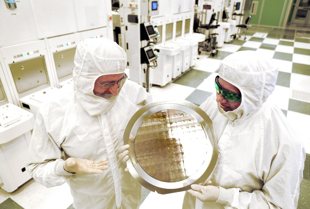
SUNY College of Nanoscale Science and Engineering's Michael Liehr, left, and IBM's Bala Haranand look at wafer comprised of 7nm chips on Thursday, July 2, 2015, in a NFX clean room Albany. Several 7nm chips at SUNY Poly CNSE on Thursday in Albany. (Darryl Bautista/Feature Photo Service for IBM)

Microelectronics products are ubiquitous. Simply, they are everywhere and the applications cut across industries. There seems to be no field where the technology has not transformed. In the pyramid of technology creation, microelectronics is positioned at the upstream level. Its advancements affect other technologies. It is safe to say that if there is no innovation in microelectronics, the ICT industry will stall and will eventually fade in style. The products come in various sizes and forms, the unnoticeable motor controller in the ‘toy train’ to the sophisticated microchips deployed in critical life saving tools used in hospital operating rooms.

Microelectronics industry (or better, electronics industry) has evolved over many decades. The era of vacuum tubes before Shockley invented the transistor at Bell Labs. The era of using discrete components-using (external) wires to join capacitors, resistors, diodes and other components together to form circuit. The problems and limitations of these ‘mouse-trap’ circuit boards were obvious. With those wires, the problems of noise (capacitive, inductive, etc) are exacerbated. The result was low performance electronic systems.

Around 1957, a Texas Instrument engineer, Jack Kilby, figured out how to make circuits without the need of using these external wires that degrade performance. He was able to help introduce a way to make all the components, resistors, transistors, capacitors, etc on the same die (substrates or simply a piece of processed silica where the circuit patterns are formed, cut them apart and you have chips). In other words, he integrated the processes of making all the components used in making circuits and eliminated the need of making them separately (as in discrete systems) and then having to solder them together with wires later. His idea, gave him a Nobel Prize, transformed the electronic industry. Not only did his idea help the improvement of performance, it also reduced the cost of making the systems. It makes sense since all the components could be fabricated virtually at the same ‘time’ with better control on process, technology and other issues which could deviate from time to time if all the units have to be made individually. Also, the products become more compact as all the components are ‘one’ and packaged alike. In most cases, the cost of developing one IC (integrated circuit) that contains 100 components could compete with the cost of developing one component. Before integration, that will be 100x cost.

Kilby’s invention helped advanced the field and gave us a new industry, microelectronics. The change from electronics to microelectronics has to do with the small dimensions of the components which are used in engineering the systems. Transistor dimensions are usually given in microns (10^-6). We are moving into the nanometer regime right now as in few years, the dimensions will be primarily dominated in the nanometer regime for state of the art designs. Nanoelectronics! Sounds familiar?

Nonetheless, let us not get carried away by history. With the advent of integrated circuits, and subsequent development of CMOS (complementary metal oxide semiconductor) technologies, there has been remarkable success in the number of application specific integrated chips (ASIC). (Let me explain in steps: CMOS is a type of transistor that works on filed effect dynamics (more on this later). ASIC is a type of chip or microchip that is designed with a specific function or application in mind; contracts with field programmable gate arrays (FPGA) which can be programmed for many different applications). Interestingly, FPGA or programmable controllers have integrated circuits that enable them to be used. The design of integrated circuit is exciting, but it is extremely knowledge-intensive. It requires mastery.

Integrated circuits are circuits that could contain millions of transistors and other circuit elements on a single die (a piece of silicon that contains active devices and input and output interfaces). They are made on special materials called semiconductors with silicon and gallium arsenide (GaAs) the most common. Its evolution is a major milestone in the history of modern industry as it has driven a revolution in computing capability due to a long trend in performance, density gains, and cost with scaling. Remarkably, these circuits could be made using different technologies. But over time, CMOS has become the industry de-facto and the most prevalent method of choice. Its major advantages over other technologies are its ease of integration of circuit components and low static power consumption. This is the main technology used to make analog-to-digital converters, micro-controllers, FPGA (an integrated circuit that contains an array of identical cells with programmable interconnections), microprocessors and host of others that are used while developing entertainment hardware. Its continuous improvements has driven reduction in size of game gadgets, better performance, more efficient battery management for battery operated devices, cost as well as hardware ergonomics.

Integrated circuit could be digital, analog or mixed signal (a combination of both analog and digital). While the digital chip involves designing at logic levels of 1 and 0, the analog is based on continuous signal. Besides, sequencing and communication synchronization on chip could be done by use of globally distributed clocks for synchronous designs or local handshaking variables for asynchronous designs. Between these two methods, the former is the more common method. However, issues like switching delay, complexity management and clock distributions, which may place limitation on synchronous chip performance with an acceptable level of reliability as technology is scaled down, had stimulated interests in the study of asynchronous systems. Asynchronous chips are known as self timed circuits since they do not use clocks but rather use local variables that perform the functions of handshaking requests and acknowledgements. Design of asynchronous digital system involves an entirely different concept when compared to synchronous design. The idea of clockless system introduces so many design parameters, which must be tracked as the requests, and acknowledgements signals are generated and routed. The initial stage of asynchronous system development would interest a computer scientist because of enormous digital “coding” that describes level of system abstraction.

In the next blog, we will examine a typical design flow for an integrated circuit.

tekedia – The waves Of Technology Launched

0

Fasmicro is the parent company of tekedia.

We are a team of engineers, policy experts and economists who are poised to use emerging technology diffusion to create the next future in Africa, starting from Nigeria. In our team are doctoral engineering graduates, post-graduate economists, hands-on experienced engineers, among others. We have a team of professionals that are leaders in their respective fields. They hold patents and are technology creators.

When clients engage us, we partner with them to deliver novel and customized solutions that will enhance their competitive advantages. We provide new insights driven by analytical vigor to provide tangible and measurable results that will position our partners and make them more capable. That capability could be anywhere: schools, business or governments.

Few firms in Nigeria and indeed Africa could match our international networks in this field. So we know when to ask for new ideas from our partners across the globe. We are structured into two divisions: the core microelectronics & embedded solutions, and ICT.

Our Mission

We seek to become change agents that will help deliver the next future in Nigeria and indeed Africa through effective technology penetration.

Our Competitive Edge
Fasmicro has managerial and technical skills to mobilize and combine the best mix of people, processes and tools to deliver high performance results with total commitment to quality.
Our Core Values
We are built under technical excellence and integrity, dependability and respect of man and society. For us, business is a partnership and we put society and clients ahead of us. We are anchored to build a better society even as we drive superior value for our partners.

Unique Capabilities
Fasmicro provides innovative skills in strategy, project management, and technical capabilities. Our areas of technical education and training specialty include computing, electronics, embededded solutions, and mobility with particular focus on microelectronics and semiconductors.

Our clients are universities, governments, government labs/agencies, civil societies, NGOs, intergovernmental organizations (like World Bank, IFC, African Union, etc), individuals, and companies. We are based in Lagos and Owerri, and fully registered with the CAC Nigeria (RC908703). Our web servers are in United States.

3AL Is A Social Network With eCommerce Integration In Nigeria

0

3AL is a personalized business networking portal, where individuals can buy and sell online. Consider it a social network like Facebook with e-commerce capability like eBay. That is why they use the slogan “Make Money, Make Friends”.


It remains to be seen how these companies that continue to build business models on the web will make money in Nigeria and become really big companies. The simple fact is: Nigeria does not do much online because the payment system is still primitive. But anyone that figures it out will see immense opportunities in the nation.