DD
MM
YYYY

PAGES

DD
MM
YYYY

spot_img

PAGES

Home Blog Page 7668

How Microchips Are Done – Major Steps Involved In Integrated Circuits Design And Development

0

The process of chip design is very complex and its understating requires many years of study and practical experience. From a digital integrated circuit design perspective, it could be divided into different hierarchies or stages where the problems are examined at several different levels: system design, logic design, circuit design, layout design, fabrication and testing. These steps are not necessarily sequential; interactions are done in practice to get things right.

System Design: This stage provides the specifications and main operations of the chip. It examines such issues like chip area, power, functionality, speed, cost and other design factors while setting these specifications. Sometimes, the resources available to the designer could act as a constraint during this stage.

For instance, a designer may like to design a chip to work at 1.2V, but available process technology can only support a voltage of 5V. In this situation, the designer has to adjust these specifications to satisfy the available tools. It is always a good habit to understand the process technology available before system design and specifications. Process technology is basically the specific foundry technology rules where the chip would be fabricated. Typical examples are AMI 0.5um, TSMC 0.35um and IBM 0.13um. A design based on one process technology is unique to that process and accordingly should be fabricated in a foundry that supports that process. At the system design level, the main sections of the system are illustrated with block diagrams, with no details on the contents of the blocks. Only the input and output characteristics of the sections are detailed.

Logic Design: At this stage, the designer implements the logic networks that would realize the input and output characteristics specified in the previous stage. This is generally made of logic gates with interconnecting wires that are used to realize the design.

Circuit Design: Circuit design involves the translation of the various logic networks into electronic circuitries using transistors. These transistors are switching devices whose combinations are used to realize different logic functions. The design is tested using computer aided design (CAD) tools and comparisons are made between the results and the chip specifications.

Through these results, the designer could have an idea of the speed, power dissipation, and performance of the final chip. An idea of the size of the chip is also obtained at this stage since the number of transistors would determine the area of the chip. Experienced designers optimize many design variables like transistor sizes, transistor numbers, and circuit architecture to reduce delay, power consumption, and latency among others. The length and width of the transistors must obey the rules of the process technology.

Layout Design: This stage involves the translation of the circuit realized in the previous stage into silicon description through geometrical patterns aided by CAD tools. This translation process follows a process rule that specifies the spacing between transistors, wire, wire contacts, and so on. Violation of these rules results to malfunctioning chips after fabrication. Besides, the designer must ensure that the layout design accurately represents the circuit design and that the design is free of errors. CAD tools enable checks for errors and also incorporate ways of comparing layout and circuit designs provided in form of Layout Versus Schematic (LVS) checks. When errors are reported, the designer has to effect the corrections.

A vital fundamental stage in layout design is Extraction, which involves the extraction of the circuit schematic from the layout drawings. The extracted circuit provides information on the circuit elements, wires, parasitic resistance and capacitance (a parasitic device is an unbudgeted device that inserts itself due to interaction between nearby components). With the aid of this extracted file, the electronic behavior of the silicon circuit is simulated and it is always a good habit to compare the results with the system specification since this is one of the final design stages before a chip is sent to the foundry.

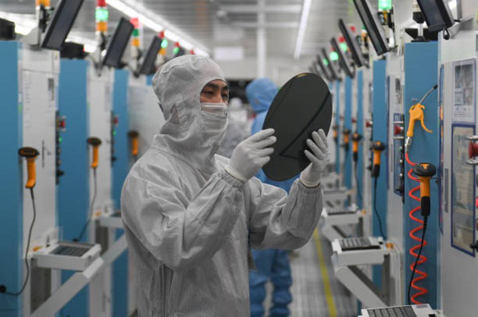
Fabrication: Upon satisfactory verification of the design, the layout is sent to the foundry where it is fabricated. The process of chip fabrication is very complex. It involves many stages of oxidation, etching, photolithography, etc. Typically, the fabrication process translates the layout into silicon or any other semiconductor material that is used. The result is bonded with pins for external connections to circuit boards.

Fabrication process uses photolithographic masks, which define specific patterns that are transferred to silicon wafers (the initial substrate used to fabricate integrated circuits) through a number of steps based on the process technology. The starting material, the wafer, is oxidized to create insulation layer in the process. It is followed by photolithographic process, which involves deposition of photoresist on the oxidized wafer, exposure to ultra-violet rays to form patterns and etching for removal of materials not covered by photoresist. Ion implantation of the p+ or n+ source/drain region and metallization to form contacts follow afterwards. The next stage is cutting the individual chip from the die.

For external pin connection, bonding is done. It is important to emphasize that this process steps could be altered in any order to achieve specific goals in the design process. In addition, many of these functions are done many times for very complex chips. Over the years, other methods have emerged. A notable one is the use of insulators (like sapphire) as starting materials instead of semiconductor substrate (the silicon on which active devices are implanted) to build the transistors. This method called Silicon on Insulator (SOI) minimizes parasitic in circuits and enable the realization of high speed and low power dissipation chips.

Testing: The final stage of the chip development is called testing. Electronic equipment like oscilloscopes, probes, pattern generators and logic analyzers are used to measure some parameters of the chip to verify its functionalities based on the stated specifications. It is always a good habit to test for various input patterns for a fairly long time in order to discover possible performance degradation, variability, or failures. Sometimes, fabricated chip test results deviate from simulated results. When that occurs, depending on application, the designer could re-engineer the circuit for improvement and error corrections. The new design should be fabricated and tested at the end.

Intel Teach And 1:1 Learning School Program Goes To Work In Nigeria

0

Intel Teach and 1:1 learning school program is a public private partnership initiative created by Intel aimed at  schools to be ready for jobs after graduations.


The Intel® Teach Program improves teacher effectiveness through professional development, helping teachers integrate technology into their lessons and promoting students’ problem-solving, critical thinking, and collaboration skills. With more than 9 million teachers trained in over 60 countries, Intel Teach is the largest, most successful program of its kind.


In Nigeria, Intel Teach  was commissioned by Intel’s Vice President and General Manager, Europe Middle East and Africa (EMEA) Mr. Christian Morale. During his working visit to Lagos State government, Intel Teach and 1:1 donated about 50 Classmate PC computers to the government.  According to Mr. Morale, Intel over the years has been a strong supporter and advocate of ICT in education.


Speaking with newsmen, he noted that “Intel is committed to the goal of reaching the next 3billon people worldwide and Nigeria is a critical part of this new thinking,”. He reiterated Intel’s readiness for continued support and to partnership with the Federal Ministry of Education and State governments, and other partners to train teachers on how to integrate technology into the classroom, thereby making teaching and learning much easier and interesting.


“Intel supports both multinational and Nigerian partners in ensuring an all round development and reach of technology in all spheres of life in Nigeria.”

ITNewsAfrica List Of “Top 10 African Women in ICT”

0


In honour of women’s day in South Africa, ITNewsAfrica is profiling 10 leading women who have made significant contributions to Africa’s Information Communication Technology (ICT) sector and occupy high profile positions in this fast paced, and sometimes cut throat industry.


Here’s our list of top 10 African women in ICT.

1. Nombulelo Moholi

Nombulelo was appointed Telkom SA CEO in March 2011 after a lengthy evaluation process.


2. Thoko Mokgosi-Mwantembe

Thoko is the CEO of Kutana Investments Group.


3. Felleng Sekha

Felleng is a non- executive director of Business Connexion, a South African black owned ICT company.


4. Zandile Mbele

Zandile was appointed as Executive: Public Sector for Internet Solutions in 2010 and as Executive Director of Transformation for the Group in 2008.


5. Dr. Sebiletso Mokone-Matabane

Dr. Sebiletso Mokone-Matabane has 25 years experience in the broadcasting, film and telecommunications sectors in the US and in South Africa.


6. Doreen Ramphaleng-Motlaleng

Doreen Ramphaleng-Motlaleng is the MD of Infomatix, a software technology company based in Gaborone, Botswana.


7. Betty Mwangi-Thuo

Betty Mwangi-Thuo joined Safaricom in December 2007 and is charged with managing the New Products Division comprising the globally acclaimed M-PESA business and Safaricom’s Value Added Service roadmap for product innovation and GSMA projects.


8. Isis Nyong’o

Isis Nyong’o is InMobi’s Vice President and Managing Director for Africa.


9. Funke Opeke

Funke Opeke leads Main One Cable Company in Nigeria.


10. Angela Gahagan

Angela Gahagan is the MTN Business managing executive and a twice-nominated candidate for the Business Woman of the Year award.


Some Of Our Books On Electrochemistry, Nanotechnology, Microelectronics And Innovation

0


Books On Sale Right Now

Nanotechnology and Microelectronics: Global Diffusion, Economics and Policy provides comprehensive research and case studies on the issues surrounding technology transfer and diffusion, trends and developments, and economics and policies as they relate to these technologies. This book serves as a resource for academics, students, policy-makers and professionals interested in advancing their knowledge of nanotechnology and microelectronics.

Electrochemical Impedance Spectroscopy: Corrosion Behavior Application

Many applications in motorcontrollers, bio-acquisition systems and energy cells balancers require reconfigurable and adaptive architectures to mitigate environmental perturbations in real time. The complexity of designing such systems is challenging, requiring robust architectures. This book provides a multimode paradigm, such that performance parameters can be adjusted using closed loop adaptation driven on sensory data from the environment. It presents mixed signal integrated System-on-Chip microsystems, which combine on-chip reconfigurable and adaptive circuit capabilities to deliver precise control signals to driver networks/electrodes. A broad applicable concept, is demonstrated by realizing controllers for surgical robots that provide performance metrics needed to manipulate delicate tissues while minimizing damage during minimal invasive surgery. Also, a single-chip/biochip for biosignals like EEG (brain), EOG (eye), ECG (heart), EMG (muscle) and neural recordings, and precision analog front-ends that support cells monitoring, variation detection, overcurrent protection and equalization are presented. The book is written for professionals and the entire academic community.


To buy at Amazon.com, click here.


Product Details


N. Ekekwe, Adaptive Application-Specific Instrumentation and Control Microsystems: MotorControllers, BioAcquisition Systems & Battery Cells Balancers, LAP, Koln, Germany, 2009.

In the first half of the twentieth century, corrosion engineers and material scientists used techniques such as salt spray and weight loss as their major methods of evaluating corrosion rates. Despite their reliabilities, these techniques are complex and time-consuming. With time, a new method, electrochemical impedance spectroscopy (EIS), has emerged to become firmly established as de facto method of evaluating corrosion behavior. This popularity has directly followed the widespread use of impedance techniques in fundamental and applied electrochemistry, and materials science. In this book, EIS is explained, qualitatively and quantitatively, and its applications to corrosion behavior of metallic structures are discussed. Because the corrosion of carbon steel and aluminum is a major infrastructure degradation problem in practically all industries, including the chemical, mineral, materials, and petrochemical industries world-wide, EIS based corrosion experiments were conducted with these metals towards developing models that will guide structural continuity management. The book is written for professionals and the entire academic community


To buy, visit Amazon.com, click here.


Co-Creation Hub Nigeria Partners With World Bank And NASA For Waterhackathon

0

October 21st to 23rd, 2011 is the period for the global WaterHackathon, an event designed with a simple mission: solve global water problems. Co-Creation Hub Nigeria will be hosting the event in Nigeria through a partnership with NASA, World Bank, among others. Simply, they want to bring software experts to hack water problems out and come up with solutions.

The WaterHackathon is a two-day marathon hacking event with multiple global locations bringing together software developers from all over to hack on real-world water problems.  The WaterHackathon event is planned for Fall 2011.

Do not think far, there is software in water purification and quality. It is just that it may not be that simple as per Nigeria’s problems because the people that need water do not live in Lagos. Some are not even counted in Nigeria’s census because they are cut-off from life. Read more and get the solutions right away if you have a lot of code armor; it is software for water; yes, software!

Water is essential to sustain life and economic development. Yet the number of people without access remains daunting: 2.5 billion with no sanitation and 887 million without access to safe water. The sustainable management of water resources has acquired a new urgency in the face a global population expected to reach nine billion by 2050, economic development spurring demand for more and better food, and increased hydrological variability caused by climate change.

New ideas, better data and innovative instruments are needed to respond to this global water crisis. In search of just that, The World Bank and its partners aims to seed a new community that brings together software engineers and water experts to (1) identify critical global challenges and project specific problems in order to (2) develop software to respond to them.  Towards this, end the WaterHackathon was conceived as venue for co-creation.

Until then, we invite you to get involved.  We need water experts from around the world to define, refine and submit problem definitions on the wide-range of water issues facing developing countries today, including access to clean water and sanitation, flood management and agricultural water management and environmental pollution.

Check out the problem definition ideas and learn how to submit a water problem.

October 21st to 23rd, 2011