

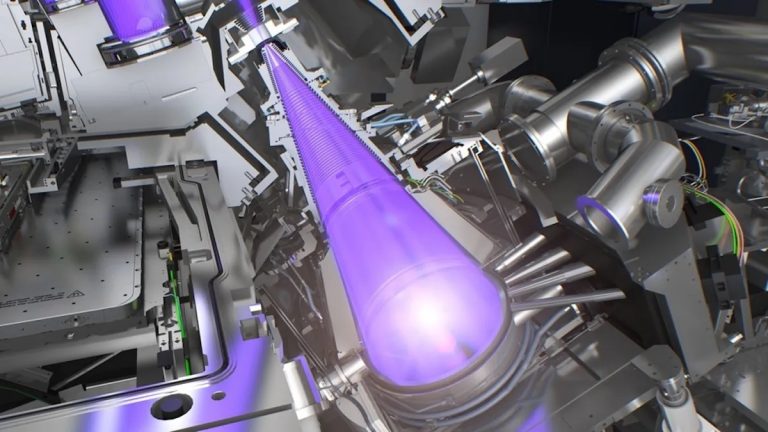
Samsung Electronics and TSMC, the world’s two largest chipmakers, have committed to using ASML’s next-generation High-NA extreme ultraviolet lithography machines, strengthening the Dutch equipment maker’s position at the center of the global semiconductor industry’s race to produce advanced chips.
The commitments provide ASML with greater visibility into demand for its most sophisticated lithography technology at a time when chipmakers are investing heavily to keep pace with the rapidly increasing computational requirements of artificial intelligence.
ASML’s EUV lithography systems are among the most critical and expensive machines in semiconductor manufacturing. They use extreme ultraviolet light to print extraordinarily fine circuit patterns onto silicon wafers, allowing chipmakers to build smaller and more sophisticated transistor structures.
Register for the next Tekedia Mini-MBA.
Register for Tekedia AI in Business Masterclass.
Join Tekedia Capital Syndicate and co-invest in great global startups.
High-NA EUV represents the next generation of the technology, using a higher numerical aperture to print smaller and more intricate patterns with greater precision. Each machine can cost around $400 million.
Samsung, one of the world’s largest memory-chip manufacturers, said it plans to use High-NA EUV machines for DRAM production from 2028.
The company said the technology would allow it to “extend the DRAM scaling roadmap” while improving manufacturing efficiency.

The move is seen as a game-changer for the memory industry, where manufacturers are under pressure to increase density and performance as demand for high-bandwidth memory and other advanced components rises alongside AI computing.
TSMC, the world’s largest contract chipmaker, said it would deploy High-NA EUV for advanced logic chips and expects its use of the technology to increase. The Taiwanese company said adoption would be driven “primarily by the increasingly complex transistor architectures required for AI applications.”
The commitments from Samsung and TSMC illustrate how the AI boom is affecting the semiconductor industry well beyond demand for processors.

Advanced AI systems require chips containing large numbers of transistors, while improvements in performance and energy efficiency depend on manufacturers continuing to shrink and refine those transistor structures.
That is making lithography one of the industry’s most important technological bottlenecks.
ASML is effectively the sole supplier of the world’s most advanced EUV lithography systems, giving it an unusually powerful position in the semiconductor equipment industry. The transition to High-NA EUV is therefore being closely watched by investors as a potential new growth cycle for the company.
Barclays said in a note Tuesday that the announcements “should provide more visibility on adoption which has been a key debate,” describing the developments as “a positive.”
ASML shares were flat to slightly lower in early Amsterdam trading on Tuesday, even as investors assess the implications of the commitments for future equipment demand.
The stock has risen about 120% over the past year, reflecting expectations that sustained investment in AI infrastructure will translate into greater spending on advanced semiconductor manufacturing equipment.
Samsung and TSMC join Intel
Samsung and TSMC now join Intel as customers for ASML’s High-NA machines. In July, ASML said Intel was already using High-NA EUV technology for advanced chip manufacturing, making the three leading semiconductor manufacturers early adopters of the technology.
The commitments are necessary because High-NA EUV machines are substantially more expensive and technically demanding than previous-generation EUV systems. Their commercial success therefore depends on whether the world’s leading chipmakers believe the additional manufacturing capability justifies the enormous investment.
ASML has not provided a recent forecast for the number of High-NA machines it expects to sell. However, the company has said it plans to increase its overall EUV capacity by about 30% in 2027.
Barclays analysts said the Samsung and TSMC announcements should improve ASML’s ability to plan future capacity.
“We see ASML with a significant decision ahead on whether to further expand EUV capacity than the recently expanded targets it has already given. Demand is clearly strong,” the analysts said.
That creates an important strategic decision for ASML. Expanding production too aggressively could leave the company with excess capacity if High-NA adoption takes longer than expected. Moving too slowly, however, could constrain sales at a time when AI-related semiconductor investment is accelerating.
The latest commitments tilt the balance toward stronger demand visibility.
Samsung and TSMC are also joining ASML in an industry initiative aimed at advancing next-generation 12-inch photomask technology, replacing the current 6-inch format. Photomasks function essentially as stencils in semiconductor manufacturing. They contain the patterns that are transferred onto silicon wafers during lithography and are therefore a critical part of the chip production process.
ASML said larger photomasks could improve productivity and reduce chipmaking costs.
The development highlights another aspect of the industry’s transition to more advanced manufacturing: progress is not limited to the lithography machine itself. Chipmakers and equipment suppliers are also redesigning surrounding processes to make complex production economically viable.
For Samsung and TSMC, the ability to manufacture more advanced chips efficiently will become more important as the cost of leading-edge fabrication rises. The adoption of High-NA EUV by Samsung, TSMC and Intel provides an early indication that the technology is moving beyond the experimental stage toward broader commercial deployment.
The timetable is still gradual. Samsung’s planned DRAM adoption from 2028 and TSMC’s expectation of increasing use suggest that High-NA EUV will become a progressively larger part of advanced chip manufacturing rather than replacing existing EUV systems overnight.
That transition could nevertheless create a substantial new equipment market for ASML.
The economics are compelling for chipmakers if High-NA technology allows them to produce more sophisticated transistor structures with fewer processing steps, higher yields, or better performance. The $400 million price tag for an individual machine becomes easier to justify if it reduces other manufacturing costs or enables chips that cannot be produced economically with older technology.
Therefore, the announcements represent more than customer commitments. They provide ASML with evidence that the world’s leading chipmakers are preparing to spend heavily on the next generation of lithography as AI pushes semiconductor designs toward greater complexity.