Microelectronics products are ubiquitous. Simply, they are everywhere and the applications cut across industries. There seems to be no field where the technology has not transformed. In the pyramid of technology creation, microelectronics is positioned at the upstream level. Its advancements affect other technologies. It is safe to say that if there is no innovation in microelectronics, the ICT industry will stall and will eventually fade in style. The products come in various sizes and forms, the unnoticeable motor controller in the ‘toy train’ to the sophisticated microchips deployed in critical life saving tools used in hospital operating rooms.
Microelectronics industry (or better, electronics industry) has evolved over many decades. The era of vacuum tubes before Shockley invented the transistor at Bell Labs. The era of using discrete components-using (external) wires to join capacitors, resistors, diodes and other components together to form circuit. The problems and limitations of these ‘mouse-trap’ circuit boards were obvious. With those wires, the problems of noise (capacitive, inductive, etc) are exacerbated. The result was low performance electronic systems.
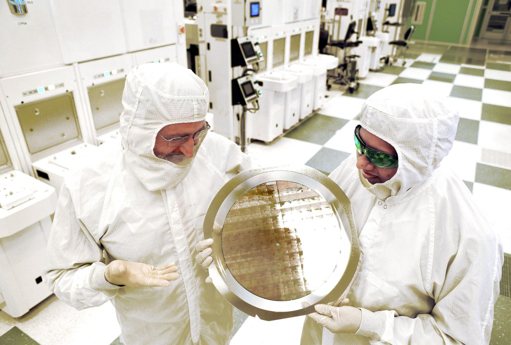
Around 1957, a Texas Instrument engineer, Jack Kilby, figured out how to make circuits without the need of using these external wires that degrade performance. He was able to help introduce a way to make all the components, resistors, transistors, capacitors, etc on the same die (substrates or simply a piece of processed silica where the circuit patterns are formed, cut them apart and you have chips). In other words, he integrated the processes of making all the components used in making circuits and eliminated the need of making them separately (as in discrete systems) and then having to solder them together with wires later. His idea, gave him a Nobel Prize, transformed the electronic industry. Not only did his idea help the improvement of performance, it also reduced the cost of making the systems. It makes sense since all the components could be fabricated virtually at the same ‘time’ with better control on process, technology and other issues which could deviate from time to time if all the units have to be made individually. Also, the products become more compact as all the components are ‘one’ and packaged alike. In most cases, the cost of developing one IC (integrated circuit) that contains 100 components could compete with the cost of developing one component. Before integration, that will be 100x cost.
Kilby’s invention helped advanced the field and gave us a new industry, microelectronics. The change from electronics to microelectronics has to do with the small dimensions of the components which are used in engineering the systems. Transistor dimensions are usually given in microns (10^-6). We are moving into the nanometer regime right now as in few years, the dimensions will be primarily dominated in the nanometer regime for state of the art designs. Nanoelectronics! Sounds familiar?
Nonetheless, let us not get carried away by history. With the advent of integrated circuits, and subsequent development of CMOS (complementary metal oxide semiconductor) technologies, there has been remarkable success in the number of application specific integrated chips (ASIC). (Let me explain in steps: CMOS is a type of transistor that works on filed effect dynamics (more on this later). ASIC is a type of chip or microchip that is designed with a specific function or application in mind; contracts with field programmable gate arrays (FPGA) which can be programmed for many different applications). Interestingly, FPGA or programmable controllers have integrated circuits that enable them to be used. The design of integrated circuit is exciting, but it is extremely knowledge-intensive. It requires mastery.
Integrated circuits are circuits that could contain millions of transistors and other circuit elements on a single die (a piece of silicon that contains active devices and input and output interfaces). They are made on special materials called semiconductors with silicon and gallium arsenide (GaAs) the most common. Its evolution is a major milestone in the history of modern industry as it has driven a revolution in computing capability due to a long trend in performance, density gains, and cost with scaling. Remarkably, these circuits could be made using different technologies. But over time, CMOS has become the industry de-facto and the most prevalent method of choice. Its major advantages over other technologies are its ease of integration of circuit components and low static power consumption. This is the main technology used to make analog-to-digital converters, micro-controllers, FPGA (an integrated circuit that contains an array of identical cells with programmable interconnections), microprocessors and host of others that are used while developing entertainment hardware. Its continuous improvements has driven reduction in size of game gadgets, better performance, more efficient battery management for battery operated devices, cost as well as hardware ergonomics.
Integrated circuit could be digital, analog or mixed signal (a combination of both analog and digital). While the digital chip involves designing at logic levels of 1 and 0, the analog is based on continuous signal. Besides, sequencing and communication synchronization on chip could be done by use of globally distributed clocks for synchronous designs or local handshaking variables for asynchronous designs. Between these two methods, the former is the more common method. However, issues like switching delay, complexity management and clock distributions, which may place limitation on synchronous chip performance with an acceptable level of reliability as technology is scaled down, had stimulated interests in the study of asynchronous systems. Asynchronous chips are known as self timed circuits since they do not use clocks but rather use local variables that perform the functions of handshaking requests and acknowledgements. Design of asynchronous digital system involves an entirely different concept when compared to synchronous design. The idea of clockless system introduces so many design parameters, which must be tracked as the requests, and acknowledgements signals are generated and routed. The initial stage of asynchronous system development would interest a computer scientist because of enormous digital “coding” that describes level of system abstraction.
In the next blog, we will examine a typical design flow for an integrated circuit.


